- 您现在的位置:买卖IC网 > PDF目录1852 > MCP1416RT-E/OT (Microchip Technology)IC PWR MOSFET DVR 1.5A SOT23-5 PDF资料下载
参数资料
| 型号: | MCP1416RT-E/OT |
| 厂商: | Microchip Technology |
| 文件页数: | 11/20页 |
| 文件大小: | 0K |
| 描述: | IC PWR MOSFET DVR 1.5A SOT23-5 |
| 标准包装: | 3,000 |
| 类型: | 低端 |
| 输入类型: | 非反相 |
| 输出数: | 1 |
| 导通状态电阻: | 6 欧姆 |
| 电流 - 峰值输出: | 1.5A |
| 电源电压: | 4.5 V ~ 18 V |
| 工作温度: | -40°C ~ 125°C |
| 安装类型: | 表面贴装 |
| 封装/外壳: | SC-74A,SOT-753 |
| 供应商设备封装: | SOT-23-5 |
| 包装: | 带卷 (TR) |
�� �
�
�MCP1415/16�
�4.4�
�Power� Dissipation�
�4.4.3�
�OPERATING� POWER� DISSIPATION�
�The� total� internal� power� dissipation� in� a� MOSFET� driver�
�is� the� summation� of� three� separate� power� dissipation�
�elements.�
�EQUATION� 4-1:�
�P� T� =� PL� +� PQ� +� P� CC�
�The� operating� power� dissipation� occurs� each� time� the�
�MOSFET� driver� output� transitions� because� for� a� very�
�short� period� of� time� both� MOSFETs� in� the� output� stage�
�are� on� simultaneously.� This� cross-conduction� current�
��EQUATION� 4-4:�
�Where:�
�P� T�
�=�
�Total� power� dissipation�
�Where:�
�P�
�CC�
�=� CC� ?� f� ?� V�
�DD�
�P� L�
�P� Q�
�P� CC�
�=�
�=�
�=�
�Load� power� dissipation�
�Quiescent� power� dissipation�
�Operating� power� dissipation�
�CC�
�f�
�=�
�=�
�Cross-conduction� constant�
�(A*sec)�
�Switching� frequency�
�4.4.1�
�CAPACITIVE� LOAD� DISSIPATION�
�V� DD�
�=�
�MOSFET� driver� supply� voltage�
�The� power� dissipation� caused� by� a� capacitive� load� is� a�
�4.5�
�PCB� Layout� Considerations�
�direct� function� of� the� frequency,� total� capacitive� load,�
�and� supply� voltage.� The� power� lost� in� the� MOSFET�
�driver� for� a� complete� charging� and� discharging� cycle� of�
��EQUATION� 4-2:�
�Proper� PCB� layout� is� important� in� high� current,� fast�
�switching� circuits� to� provide� proper� device� operation�
�and� robustness� of� design.� Improper� component�
�placement� may� cause� errant� switching,� excessive�
�voltage� ringing,� or� circuit� latch-up.� PCB� trace� loop� area�
�=� f� ?� C� ?� V�
�Where:�
�P�
�L�
�T�
�DD�
�2�
�and� inductance� must� be� minimized.� This� is�
�accomplished� by� placing� the� MOSFET� driver� directly� at�
�the� load� and� placing� the� bypass� capacitor� directly� at� the�
�f�
�C� T�
�V� DD�
�=�
�=�
�=�
�Switching� frequency�
�Total� load� capacitance�
�MOSFET� driver� supply� voltage�
�MOSFET� driver� (� Figure� 4-3� ).� Locating� ground� planes�
�or� ground� return� traces� directly� beneath� the� driver�
�output� signal� also� reduces� trace� inductance.� A� ground�
�plane� will� also� help� as� a� radiated� noise� shield� as� well� as�
�providing� some� heat� sinking� for� power� dissipated� within�
�4.4.2�
�QUIESCENT� POWER� DISSIPATION�
�the� device� (� Figure� 4-4� ).�
�The� power� dissipation� associated� with� the� quiescent�
�current� draw� depends� upon� the� state� of� the� input� pin.�
�The� MCP1415/16� devices� have� a� quiescent� current�
�draw� when� the� input� is� high� of� 0.65� mA� (typical)� and�
�0.1� mA� (typical)� when� the� input� is� low.� The� quiescent�
��EQUATION� 4-3:�
�PQ� =� ?� IQH� ?� D� +� IQL� ?� ?� 1� –� D� ?� ?� ?� VDD�
�Where:�
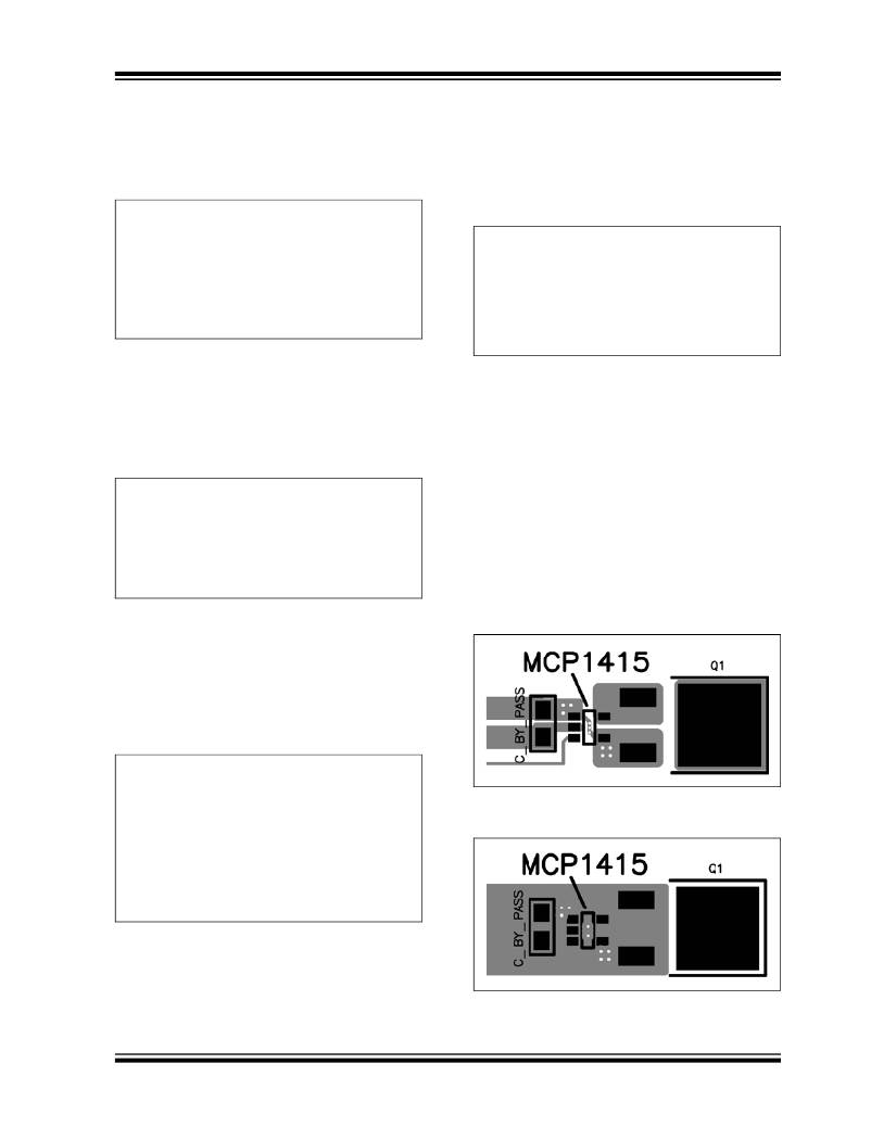
�FIGURE� 4-3:�
�Recommended� PCB� Layout�
�I� QH�
�=�
�Quiescent� current� in� the� high�
�(TOP).�
�state�
�D�
�I� QL�
�V� DD�
�=�
�=�
�=�
�Duty� cycle�
�Quiescent� current� in� the� low�
�state�
�MOSFET� driver� supply� voltage�
�FIGURE� 4-4:�
�(BOTTOM).�
�Recommended� PCB� Layout�
�?� 2008-2012� Microchip� Technology� Inc.�
�DS22092E-page� 11�
�相关PDF资料 |
PDF描述 |
|---|---|
| MCP1525-I/TO | IC VREF SERIES PREC 2.5V TO-92-3 |
| MCP1601T-I/MS | IC REG BUCK SYNC ADJ 0.5A 8MSOP |
| MCP1602-330I/MF | IC REG BUCK SYNC 3.3V 0.5A 8DFN |
| MCP1603T-080I/OS | IC REG BUCK SYNC 0.8V TSOT23-6 |
| MCP1612-ADJI/MF | IC REG BUCK SYNC ADJ 1A 8DFN |
相关代理商/技术参数 |
参数描述 |
|---|---|
| MCP1416RT-OT | 制造商:MICROCHIP 制造商全称:Microchip Technology 功能描述:Tiny 1.5A, High-Speed Power MOSFET Driver |
| MCP1416T | 制造商:MICROCHIP 制造商全称:Microchip Technology 功能描述:Tiny 1.5A, High-Speed Power MOSFET Driver |
| MCP1416T-E | 制造商:MICROCHIP 制造商全称:Microchip Technology 功能描述:Tiny 1.5A, High-Speed Power MOSFET Driver |
| MCP1416T-E/MC | 功能描述:功率驱动器IC 1.5A SNGL MOSFET Drvr RoHS:否 制造商:Micrel 产品:MOSFET Gate Drivers 类型:Low Cost High or Low Side MOSFET Driver 上升时间: 下降时间: 电源电压-最大:30 V 电源电压-最小:2.75 V 电源电流: 最大功率耗散: 最大工作温度:+ 85 C 安装风格:SMD/SMT 封装 / 箱体:SOIC-8 封装:Tube |
| MCP1416T-E/OT | 功能描述:功率驱动器IC 1.5A SNGL MOSFET Drvr RoHS:否 制造商:Micrel 产品:MOSFET Gate Drivers 类型:Low Cost High or Low Side MOSFET Driver 上升时间: 下降时间: 电源电压-最大:30 V 电源电压-最小:2.75 V 电源电流: 最大功率耗散: 最大工作温度:+ 85 C 安装风格:SMD/SMT 封装 / 箱体:SOIC-8 封装:Tube |
发布紧急采购,3分钟左右您将得到回复。