- 您现在的位置:买卖IC网 > PDF目录1852 > MCP1612-ADJI/MF (Microchip Technology)IC REG BUCK SYNC ADJ 1A 8DFN PDF资料下载
参数资料
| 型号: | MCP1612-ADJI/MF |
| 厂商: | Microchip Technology |
| 文件页数: | 13/22页 |
| 文件大小: | 0K |
| 描述: | IC REG BUCK SYNC ADJ 1A 8DFN |
| 标准包装: | 120 |
| 类型: | 降压(降压) |
| 输出类型: | 可调式 |
| 输出数: | 1 |
| 输出电压: | 0.8 V ~ 5 V |
| 输入电压: | 2.7 V ~ 5.5 V |
| PWM 型: | 电流模式 |
| 频率 - 开关: | 1.4MHz |
| 电流 - 输出: | 1A |
| 同步整流器: | 是 |
| 工作温度: | -40°C ~ 85°C |
| 安装类型: | 表面贴装 |
| 封装/外壳: | 8-VDFN 裸露焊盘 |
| 包装: | 管件 |
| 供应商设备封装: | 8-DFN-EP(3x3) |
�� �
�
�MCP1612�
�Solving� for� C:�
�5.2.6�
�COMPENSATION� COMPONENTS�
�C� =� I� C� � -----------�
�Δ� t�
�Δ� V� C�
�Where:�
�I� C� =� peak-to-peak� ripple� current�
�Δ� t� =� on-time� of� P-channel� MOSFET�
�Δ� V� C� =� output� ripple� voltage�
�An� internal� transconductance� error� amplifier� is� used� to�
�compensate� the� buck� converter.� An� external� resistor�
�(R� C� )� and� capacitor� (C� C� ),� connected� between� COMP�
�and� GND,� are� all� that� is� needed� to� provide� a� high-�
�bandwidth� loop.�
��buck� inductor� (L)� and� output� capacitor� (C� OUT� )� values.�
�There� will� also� be� some� ripple� voltage� caused� by� the�
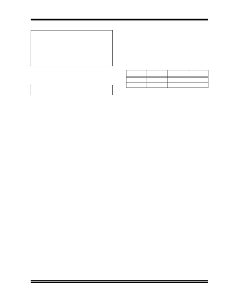
�TABLE� 5-1:�
�R� C� and� C� C� VALUES�
�ESR� of� the� capacitor.� The� ripple� is� defined� as� follows.�
�EQUATION� 5-7:�
�V� ESRRIPPLE� =� ESR� � I� C�
�L�
�3.3� μH�
�2.2� μH�
�C� OUT�
�10.0� μF�
�4.7� μF�
�R� C�
�25� k� Ω�
�10� k� Ω�
�C� C�
�1000� pF�
�1000� pF�
�For� this� example:�
�5.3�
�Printed� Circuit� Board� (PCB)�
�Layout�
�I� C� =� 165� mA�
�C� =� 4.7� μF�
�Δ� t� =� 260� ns�
�ESR� =� 8� m� Ω�
�Δ� V� C� =� (260� ns� x� 165� mA)/4.7� μF�
�Δ� V� C� =� 9.13� mV�
�V� ESRRIPPLE� =� 8� m� Ω� x� 165� mA�
�V� ESRRIPPLE� =� 1.32� mV�
�Δ� V� OUT� =� Δ� V� C� +� V� ESRRIPPLE�
�Δ� V� OUT� =� 9.13� mV� +� 1.32� mV�
�Δ� V� OUT� =� 10.45� mV�
�The� MCP1612� is� capable� of� switching� over� 1A� at�
�1.4� MHz.� As� with� all� high-frequency� switching� power�
�supplies,� good� PCB� layout� techniques� are� essential� to�
�prevent� noise� generated� by� the� switching� power-train�
�from� interfering� with� the� sensing� circuitry.�
�There� are� two� ground� pins� (P� GND� and� A� GND� )� on� the�
�MCP1612� to� separate� the� large-signal� ground� current�
�from� the� small-signal� circuit� ground.� These� two�
�grounds� should� be� kept� separate,� only� connecting� near�
�the� input� bulk� capacitor.�
�Care� must� also� be� taken� to� minimize� the� length� and�
�loop� area� of� the� large� signal� connections.� Components�
�connected� to� this� loop� consist� of� the� input� bulk�
�5.2.4�
�INPUT� CAPACITOR�
�capacitor,� V� IN� ,� P� GND� and� L� X� pins� of� the� MCP1612,� the�
�buck� inductor� and� the� output� filter� capacitor.�
�For� the� buck� topology,� the� input� current� is� pulled� from�
�the� source� and� the� input� capacitor� in� pulses.� The� size�
�of� the� input� capacitor� will� determine� the� amount� of�
�current� pulled� from� the� source.� For� most� applications,�
�a� 10� μF� ceramic� capacitor� connected� between� the�
�MCP1612’s� V� IN� and� P� GND� is� recommended� to� filter� the�
�current� pulses.� Less� capacitance� can� be� used� for�
�applications� that� have� low� source� impedance.� The�
�ripple� current� rating� for� ceramic� capacitors� are� typically�
�very� high� due� to� their� low� loss� characteristics.� Low-cost�
�electrolytic� capacitors� can� be� used,� but� their� ripple�
�current� rating� should� not� be� exceeded.�
�5.2.5�
�V� CC� INPUT�
�The� V� CC� input� is� used� to� bias� the� internal� MCP1612�
�circuitry.� A� 10� Ω� resistor� is� recommended� between� the�
�unregulated� inputs� V� IN� and� V� CC� ,� along� with� a� 0.1� μF�
�capacitor� to� ground� to� help� isolate� the� V� CC� pin� from� the�
�switching� noise.�
�?� 2005� Microchip� Technology� Inc.�
�DS21921B-page� 13�
�相关PDF资料 |
PDF描述 |
|---|---|
| MCP1624T-I/MC | IC BOOST SYNC REG PWM/PFM 8DFN |
| MCP1630-E/MS | IC REG CTRLR BST FLYBK ISO 8MSOP |
| MCP16301T-I/CHY | IC REG BUCK ADJ 0.6A SOT23-6 |
| MCP1631-E/ST | IC REG CTRLR ISO PWM CM 20-TSSOP |
| MCP1631HVT-500E/ST | IC REG CTRLR ISO PWM CM 20-TSSOP |
相关代理商/技术参数 |
参数描述 |
|---|---|
| MCP1612-ADJIMS | 制造商:MICROCHIP 制造商全称:Microchip Technology 功能描述:Single 1A, 1.4 MHz Synchronous Buck Regulator |
| MCP1612EV | 功能描述:电源管理IC开发工具 MCP1612 Synch Buck Reg Eval Brd RoHS:否 制造商:Maxim Integrated 产品:Evaluation Kits 类型:Battery Management 工具用于评估:MAX17710GB 输入电压: 输出电压:1.8 V |
| MCP1612-I/MF | 制造商:MICROCHIP 制造商全称:Microchip Technology 功能描述:Single 1A, 1.4 MHz Synchronous Buck Regulator |
| MCP1612-I/MS | 制造商:MICROCHIP 制造商全称:Microchip Technology 功能描述:Single 1A, 1.4 MHz Synchronous Buck Regulator |
| MCP1612T | 制造商:MICROCHIP 制造商全称:Microchip Technology 功能描述:Single 1A, 1.4 MHz Synchronous Buck Regulator |
发布紧急采购,3分钟左右您将得到回复。