- 您现在的位置:买卖IC网 > PDF目录4983 > MCP1703AT-3302E/MB (Microchip Technology)IC REG LDO 3.3V .25A SOT-89-3 PDF资料下载
参数资料
| 型号: | MCP1703AT-3302E/MB |
| 厂商: | Microchip Technology |
| 文件页数: | 4/30页 |
| 文件大小: | 0K |
| 描述: | IC REG LDO 3.3V .25A SOT-89-3 |
| 标准包装: | 1,000 |
| 稳压器拓扑结构: | 正,固定式 |
| 输出电压: | 3.3V |
| 输入电压: | 最高 16V |
| 电压 - 压降(标准): | 0.525V @ 250mA |
| 稳压器数量: | 1 |
| 电流 - 输出: | 250mA(最小) |
| 工作温度: | -40°C ~ 125°C |
| 安装类型: | 表面贴装 |
| 封装/外壳: | TO-243AA |
| 供应商设备封装: | SOT-89-3 |
| 包装: | 带卷 (TR) |
第1页第2页第3页当前第4页第5页第6页第7页第8页第9页第10页第11页第12页第13页第14页第15页第16页第17页第18页第19页第20页第21页第22页第23页第24页第25页第26页第27页第28页第29页第30页
�� �
�
�MCP1703A�
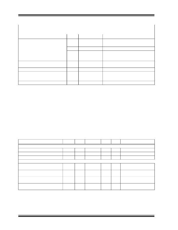
�DC� CHARACTERISTICS� (CONTINUED)�
�Electrical� Specifications:� Unless� otherwise� specified,� all� limits� are� established� for� V� IN� =� V� OUT(MAX)� +� V� DROPOUT(MAX)� ,� Note� 1� ,�
�I� LOAD� =� 1� mA,� C� OUT� =� 1� μF� (X7R),� C� IN� =� 1� μF� (X7R),� T� A� =� +25°C.� Boldface� type� applies� for� junction� temperatures,�
�T� J� (� Note� 7� )� of� -40°C� to� +125°C.�
�Parameters�
�Dropout� Voltage�
��Output� Delay� Time�
�Symbol�
�V� DROPOUT�
�T� DELAY�
�Min�
�—�
�—�
�—�
�—�
�—�
�—�
�Typ�
�330�
�525�
�625�
�750�
�—�
�600�
�Max�
�650�
�725�
�975�
�1100�
�—�
�—�
�Units�
�mV�
�mV�
�mV�
�mV�
�mV�
�μs�
�Conditions�
�I� L� =� 250� mA,� V� R� =� 5.0V�
�I� L� =� 250� mA,� 3.3V� ≤� V� R� <� 5.0V�
�I� L� =� 250� mA,� 2.8V� ≤� V� R� <� 3.3V�
�I� L� =� 250� mA,� 2.5V� ≤� V� R� <� 2.8V�
�V� R� <� 2.5V,� See� Maximum� Output�
�Current� Parameter�
�V� IN� =� 0V� to� 6V,� V� OUT� =� 90%� V� R� ,�
�R� L� =� 50� Ω� resistive�
�Output� Noise�
�e� N�
�—�
�0.3�
�μV/(Hz)� 1/2� I� L� =� 50� mA,� f� =� 1� kHz,� C� OUT� =� 1� μF�
�Power� Supply� Ripple�
�Rejection� Ratio�
�Thermal� Shutdown� Protection�
�PSRR�
�T� SD�
�—�
�—�
�35�
�150�
�—�
�—�
�dB�
�°C�
�f� =� 100� Hz,� C� OUT� =� 1� μF,� I� L� =� 10� mA,�
�V� INAC� =� 200� mV� pk-pk,� C� IN� =� 0� μF,�
�V� R� =� 5.0V�
�Note� 1:�
�2:�
�3:�
�4:�
�5:�
�6:�
�7:�
�The� minimum� V� IN� must� meet� two� conditions:� V� IN� ≥� 2.7V� and� V� IN� ≥� (V� OUT(MAX)� +� V� DROPOUT(MAX)� ).�
�V� R� is� the� nominal� regulator� output� voltage.� For� example:� V� R� =� 1.2V,� 1.5V,� 1.8V,� 2.5V,� 2.8V,� 3.0V,� 3.3V,� 4.0V,� or� 5.0V.�
�The� input� voltage� V� IN� =� V� OUT(MAX)� +� V� DROPOUT(MAX)� or� Vi� IN� =� 2.7V� (whichever� is� greater);� I� OUT� =� 100� μA.�
�TCV� OUT� =� (V� OUT-HIGH� -� V� OUT-LOW� )� x� 10� 6� /(V� R� x� Δ� Temperature),� V� OUT-HIGH� =� highest� voltage� measured� over� the�
�temperature� range.� V� OUT-LOW� =� lowest� voltage� measured� over� the� temperature� range.�
�Load� regulation� is� measured� at� a� constant� junction� temperature� using� low� duty� cycle� pulse� testing.� Changes� in� output�
�voltage� due� to� heating� effects� are� determined� using� thermal� regulation� specification� TCV� OUT� .�
�Dropout� voltage� is� defined� as� the� input� to� output� differential� at� which� the� output� voltage� drops� 2%� below� its� measured�
�value� with� an� applied� input� voltage� of� V� OUT(MAX)� +� V� DROPOUT(MAX)� or� 2.7V,� whichever� is� greater.�
�The� maximum� allowable� power� dissipation� is� a� function� of� ambient� temperature,� the� maximum� allowable� junction�
�temperature� and� the� thermal� resistance� from� junction� to� air� (i.e.,� T� A� ,� T� J� ,� q� JA� ).� Exceeding� the� maximum� allowable� power�
�dissipation� will� cause� the� device� operating� junction� temperature� to� exceed� the� maximum� 150°C� rating.� Sustained�
�junction� temperatures� above� 150°C� can� impact� the� device� reliability.�
�The� junction� temperature� is� approximated� by� soaking� the� device� under� test� at� an� ambient� temperature� equal� to� the�
�desired� junction� temperature.� The� test� time� is� small� enough� such� that� the� rise� in� the� junction� temperature� over� the� ambi-�
�ent� temperature� is� not� significant.�
��Parameters�
�Sym�
�Min�
�Typ�
�Max�
�Units�
�Conditions�
�Temperature� Ranges�
�Operating� Junction� Temperature� Range�
�Maximum� Junction� Temperature�
�Storage� Temperature� Range�
�T� J�
�T� J�
�T� A�
�-40�
�—�
�-65�
�—�
�—�
�—�
�+125�
�+150�
�+150�
�°C�
�°C�
�°C�
�Steady� State�
�Transient�
��Thermal� Resistance,� 3LD� SOT-223�
�Thermal� Resistance,� 3LD� SOT-23A�
�Thermal� Resistance,� 3LD� SOT-89�
�Thermal� Resistance,� 8LD� 2x3� DFN�
�θ� JA�
�θ� JC�
�θ� JA�
�θ� JC�
�θ� JA�
�θ� JC�
�θ� JA�
�θ� JC�
�—�
�—�
�—�
�—�
�—�
�—�
�—�
�—�
�62�
�15�
�336�
�110�
�180�
�52�
�70�
�13.4�
�—�
�—�
�—�
�—�
�—�
�—�
�—�
�—�
�°C/W�
�°C/W�
�°C/W�
�°C/W�
�EIA/JEDEC� JESD51-7�
�FR-4� 0.063� 4-Layer� Board�
�EIA/JEDEC� JESD51-7�
�FR-4� 0.063� 4-Layer� Board�
�EIA/JEDEC� JESD51-7�
�FR-4� 0.063� 4-Layer� Board�
�EIA/JEDEC� JESD51-7�
�FR-4� 0.063� 4-Layer� Board�
�Note� 1:�
�2:�
�The� maximum� allowable� power� dissipation� is� a� function� of� ambient� temperature,� the� maximum� allowable� junction�
�temperature� and� the� thermal� resistance� from� junction� to� air� (i.e.,� T� A� ,� T� J� ,� θ� JA� ).� Exceeding� the� maximum� allowable� power�
�dissipation� will� cause� the� device� operating� junction� temperature� to� exceed� the� maximum� 150°C� rating.� Sustained�
�junction� temperatures� above� 150°C� can� impact� the� device� reliability.�
�Thermal� Resistance� values� are� subject� to� change.� Please� visit� the� Microchip� web� site� for� the� latest� packaging�
�information.�
�DS25122A-page� 4�
�?� 2012� Microchip� Technology� Inc.�
�相关PDF资料 |
PDF描述 |
|---|---|
| ABM18DRMN | CONN EDGECARD 36POS .156 WW |
| AMM10DTBN-S189 | CONN EDGECARD 20POS R/A .156 SLD |
| ABM18DRMH | CONN EDGECARD 36POS .156 WW |
| MCP1703AT-3302E/CB | IC REG LDO 3.3V .25A SOT-23A-3 |
| ABM18DRMD | CONN EDGECARD 36POS .156 WW |
相关代理商/技术参数 |
参数描述 |
|---|---|
| MCP1703AT-4002E/CB | 功能描述:低压差稳压器 - LDO LOW Iq, High Vin LDO 4.0V, SOT-23A RoHS:否 制造商:Texas Instruments 最大输入电压:36 V 输出电压:1.4 V to 20.5 V 回动电压(最大值):307 mV 输出电流:1 A 负载调节:0.3 % 输出端数量: 输出类型:Fixed 最大工作温度:+ 125 C 安装风格:SMD/SMT 封装 / 箱体:VQFN-20 |
| MCP1703AT-4002E/DB | 功能描述:低压差稳压器 - LDO LOW Iq, High Vin LDO RoHS:否 制造商:Texas Instruments 最大输入电压:36 V 输出电压:1.4 V to 20.5 V 回动电压(最大值):307 mV 输出电流:1 A 负载调节:0.3 % 输出端数量: 输出类型:Fixed 最大工作温度:+ 125 C 安装风格:SMD/SMT 封装 / 箱体:VQFN-20 |
| MCP1703AT-4002E/MB | 功能描述:低压差稳压器 - LDO LOW Iq, High Vin LDO 4.0V, SOT-89 RoHS:否 制造商:Texas Instruments 最大输入电压:36 V 输出电压:1.4 V to 20.5 V 回动电压(最大值):307 mV 输出电流:1 A 负载调节:0.3 % 输出端数量: 输出类型:Fixed 最大工作温度:+ 125 C 安装风格:SMD/SMT 封装 / 箱体:VQFN-20 |
| MCP1703AT-4002E/MC | 功能描述:低压差稳压器 - LDO LOW Iq, High Vin LDO RoHS:否 制造商:Texas Instruments 最大输入电压:36 V 输出电压:1.4 V to 20.5 V 回动电压(最大值):307 mV 输出电流:1 A 负载调节:0.3 % 输出端数量: 输出类型:Fixed 最大工作温度:+ 125 C 安装风格:SMD/SMT 封装 / 箱体:VQFN-20 |
| MCP1703AT-5002E/CB | 功能描述:低压差稳压器 - LDO LOW Iq, High Vin LDO 5.0V, SOT-23A RoHS:否 制造商:Texas Instruments 最大输入电压:36 V 输出电压:1.4 V to 20.5 V 回动电压(最大值):307 mV 输出电流:1 A 负载调节:0.3 % 输出端数量: 输出类型:Fixed 最大工作温度:+ 125 C 安装风格:SMD/SMT 封装 / 箱体:VQFN-20 |
发布紧急采购,3分钟左右您将得到回复。