- 您现在的位置:买卖IC网 > PDF目录4909 > MCP1790T-5002E/EB (Microchip Technology)IC REG LDO 5V 70MA 3DDPAK PDF资料下载
参数资料
| 型号: | MCP1790T-5002E/EB |
| 厂商: | Microchip Technology |
| 文件页数: | 15/34页 |
| 文件大小: | 0K |
| 描述: | IC REG LDO 5V 70MA 3DDPAK |
| 标准包装: | 750 |
| 稳压器拓扑结构: | 正,固定式 |
| 输出电压: | 5V |
| 输入电压: | 6 V ~ 30 V |
| 电压 - 压降(标准): | 0.7V @ 70mA |
| 稳压器数量: | 1 |
| 电流 - 输出: | 70mA(最小) |
| 工作温度: | -40°C ~ 125°C |
| 安装类型: | 表面贴装 |
| 封装/外壳: | TO-263-4,D²Pak(3 引线+接片),TO-263AA |
| 供应商设备封装: | DDPAK/TO-263-3 |
| 包装: | 带卷 (TR) |
| 其它名称: | MCP1790T-5002E/EBTR |
第1页第2页第3页第4页第5页第6页第7页第8页第9页第10页第11页第12页第13页第14页当前第15页第16页第17页第18页第19页第20页第21页第22页第23页第24页第25页第26页第27页第28页第29页第30页第31页第32页第33页第34页
�� �
�
�MCP1790/MCP1791�
�4.5�
�Shutdown� (SHDN)�
�4.6�
�Low� Voltage� Shutdown�
�The� MCP1791� has� a� Shutdown� (SHDN)� input� signal�
�that� enables� or� disables� the� regulator� output� voltage.�
�When� the� SHDN� input� signal� is� greater� than� 2.40V,� the�
�regulator� output� voltage� is� enabled.� Note� that� the�
�regulator� output� may� still� be� disabled� by� the�
�undervoltage� lockout� incorporated� within� the� V� IN�
�circuitry.�
�The� value� of� the� SHDN� signal� to� put� the� regulator� into�
�Shutdown� mode� is� ≤� 0.8V.� The� SHDN� pin� is� pulled� low�
�by� an� internal� resistor.� If� the� SHDN� pin� is� left� floating,�
�the� internal� pull-down� resistor� will� put� the� regulator� into�
�shutdown� mode.�
�When� the� SHDN� input� signal� is� pulled� to� a� logic-low,� the�
�PWRGD� output� signal� will� also� go� low� and� the� regulator�
�The� MCP1790/MCP1791� incorporates� a� Low� Voltage�
�Shutdown� circuit� that� turns� off� the� output� of� the�
�regulator� whenever� the� input� voltage,� V� IN� ,� is� below� the�
�specified� turn� off� voltage,� V� OFF� .� When� the� input� voltage�
�(V� B� )� drops� below� the� differential� needed� to� provide�
�stable� regulation,� the� output� voltage� (V� REG� )� shall� track�
�the� input� down� to� approximately� +4.00V.� The� regulator�
�will� turn� off� the� output� at� this� point.�
�The� output� will� turn� on� when� V� IN� rises� above� the� V� ON�
�value� specified� in� the� data� sheet.� This� feature� is�
�independent� of� the� Shutdown� input� signal� (SHDN)� that�
�is� provided� for� external� regulator� control.� If� the� SHDN�
�input� signal� is� active� (LOW),� then� the� output� of� the�
�regulator� shall� be� disabled� regardless� of� input� voltage.�
�will� enter� a� low� quiescent� current� state� where� the�
�typical� quiescent� current� is� 10� μA.� There� is� a� short� time�
�TABLE� 4-1:�
�SHUTDOWN� LOGIC�
�delay� (approximately� 400� ns)� when� the� SHDN� input�
�signal� transitions� from� high-to-low� to� p� reven� t� signal�
�noise� from� disabling� the� regulator.� The� SHDN� pin� will�
�ignore� low-going� pulses� that� are� up� to� 400� ns� in� pulse�
�width.� If� the� SHDN� input� is� pulled� low� for� more� than�
�400� ns,� the� regulator� will� enter� Shutdown� mode.� This�
�small� bit� of� filtering� helps� to� reject� any� system� noise�
�V� IN�
�<� V� OFF�
�<� V� OFF�
�>� V� ON�
�>� V� ON�
�SHDN�
�L�
�H�
�L�
�H�
�V� OUT�
�OFF�
�OFF�
�OFF�
�ON�
�spikes� on� the� SHDN� input� signal.�
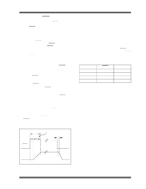
�On� the� rising� edge� of� the� SHDN� input,� the� shutdown�
�4.7�
�Output� Capacitor�
�circuitry� will� have� a� 100� μs� delay� before� allowing� the�
�regulator� output� to� turn� on.� This� delay� helps� to� reject�
�any� false� turn-on� signals� or� noise� on� the� SHDN� input�
�signal.� After� the� 100� μs� delay,� the� regulator� will� start�
�charging� the� output� capacitor� as� the� regulator� output�
�voltage� rises� from� 0V� to� its� final� regulated� value.� The�
�charging� current� will� be� limited� by� the� short� circuit�
�current� value� of� the� device.� If� the� SHDN� input� signal� is�
�pulled� low� during� the� 100� μs� delay� period,� the� timer� will�
�be� reset� and� the� delay� time� will� start� over� again� on� the�
�next� rising� edge� of� the� SHDN� input.� The� total� time� from�
�the� SHDN� input� going� high� (turn-on)� to� the� regulator�
�output� being� in� regulation� shall� typically� be� 200� μs�
�(100� μs� +� 100� μs)� for� a� C� LOAD� =� 1.0� μF.�
�The� MCP1790/MCP1791� requires� a� minimum� output�
�capacitance� of� 1� μF� tantalum� or� electrolytic�
�capacitance.� The� minimum� value� for� ceramic�
�capacitors� is� 4.7� μF.� The� regulator� is� stable� for� all� three�
�types� of� capacitors� from� 4.7� μF� to� 1000� μF� (see�
��be� used� with� a� 1� μF� ceramic� output� capacitor� if� a�
�0.300� Ω� resistor� is� placed� in� series� with� the� capacitor.�
�The� low� ESR� and� corresponding� pole� of� the� ceramic�
�capacitor� causes� the� instability� below� 4.7� μF.�
�The� Equivalent� Series� Resistance� (ESR)� of� the� output�
�capacitor� must� be� no� greater� than� 3� ohms.� The� output�
�capacitor� should� be� located� as� close� to� the� regulator�
�output� as� is� practical.� Ceramic� materials� X7R� and� X5R�
�have� low� temperature� coefficients� and� are�
�100� μs�
�TOR�
�100 μs�
�C� LOAD� C� HARGING� T� IME�
�400� ns� (typ)�
�recommended� because� of� their� size,� cost� and�
�environmental� robustness� qualities.�
�SHDN�
�V� OUT�
�C� LOAD� =� 1.0� μF�
�FIGURE� 4-2:�
�Diagram.�
�Shutdown� Input� Timing�
�?� 2010� Microchip� Technology� Inc.�
�DS22075B-page� 15�
�相关PDF资料 |
PDF描述 |
|---|---|
| MCP1791T-3002E/ET | IC REG LDO 3V 70MA 5DDPAK |
| MCP1791T-3302E/ET | IC REG LDO 3.3V 70MA 5DDPAK |
| MCP1791T-5002E/ET | IC REG LDO 5V 70MA 5DDPAK |
| RCC40DRSD-S273 | CONN EDGECARD 80POS DIP .100 SLD |
| EYM43DTMT-S189 | CONN EDGECARD 86POS R/A .156 SLD |
相关代理商/技术参数 |
参数描述 |
|---|---|
| MCP1791-3002E/DC | 功能描述:低压差稳压器 - LDO HI VLTG LDO 50 mA RoHS:否 制造商:Texas Instruments 最大输入电压:36 V 输出电压:1.4 V to 20.5 V 回动电压(最大值):307 mV 输出电流:1 A 负载调节:0.3 % 输出端数量: 输出类型:Fixed 最大工作温度:+ 125 C 安装风格:SMD/SMT 封装 / 箱体:VQFN-20 |
| MCP1791-3002E/ET | 功能描述:低压差稳压器 - LDO HI VLTG LDO 50 mA RoHS:否 制造商:Texas Instruments 最大输入电压:36 V 输出电压:1.4 V to 20.5 V 回动电压(最大值):307 mV 输出电流:1 A 负载调节:0.3 % 输出端数量: 输出类型:Fixed 最大工作温度:+ 125 C 安装风格:SMD/SMT 封装 / 箱体:VQFN-20 |
| MCP1791-3302E/DC | 功能描述:低压差稳压器 - LDO HI VLTG LDO 50 mA RoHS:否 制造商:Texas Instruments 最大输入电压:36 V 输出电压:1.4 V to 20.5 V 回动电压(最大值):307 mV 输出电流:1 A 负载调节:0.3 % 输出端数量: 输出类型:Fixed 最大工作温度:+ 125 C 安装风格:SMD/SMT 封装 / 箱体:VQFN-20 |
| MCP1791-3302E/ET | 功能描述:低压差稳压器 - LDO HI VLTG LDO 50 mA RoHS:否 制造商:Texas Instruments 最大输入电压:36 V 输出电压:1.4 V to 20.5 V 回动电压(最大值):307 mV 输出电流:1 A 负载调节:0.3 % 输出端数量: 输出类型:Fixed 最大工作温度:+ 125 C 安装风格:SMD/SMT 封装 / 箱体:VQFN-20 |
| MCP1791-5002E/DC | 功能描述:低压差稳压器 - LDO HI VLTG LDO 50 mA RoHS:否 制造商:Texas Instruments 最大输入电压:36 V 输出电压:1.4 V to 20.5 V 回动电压(最大值):307 mV 输出电流:1 A 负载调节:0.3 % 输出端数量: 输出类型:Fixed 最大工作温度:+ 125 C 安装风格:SMD/SMT 封装 / 箱体:VQFN-20 |
发布紧急采购,3分钟左右您将得到回复。