- 您现在的位置:买卖IC网 > PDF目录4989 > MCP1804T-C002I/OT (Microchip Technology)IC REG LDO 12V .15A SOT23-5 PDF资料下载
参数资料
| 型号: | MCP1804T-C002I/OT |
| 厂商: | Microchip Technology |
| 文件页数: | 16/32页 |
| 文件大小: | 0K |
| 描述: | IC REG LDO 12V .15A SOT23-5 |
| 标准包装: | 1 |
| 稳压器拓扑结构: | 正,固定式 |
| 输出电压: | 12V |
| 输入电压: | 最高 28V |
| 电压 - 压降(标准): | 0.65V @ 100mA |
| 稳压器数量: | 1 |
| 电流 - 输出: | 150mA(最小) |
| 工作温度: | -40°C ~ 85°C |
| 安装类型: | 表面贴装 |
| 封装/外壳: | SC-74A,SOT-753 |
| 供应商设备封装: | SOT-23-5 |
| 包装: | 标准包装 |
| 产品目录页面: | 668 (CN2011-ZH PDF) |
| 其它名称: | MCP1804T-C002I/OTDKR |
第1页第2页第3页第4页第5页第6页第7页第8页第9页第10页第11页第12页第13页第14页第15页当前第16页第17页第18页第19页第20页第21页第22页第23页第24页第25页第26页第27页第28页第29页第30页第31页第32页
�� �
�
�MCP1804�
�3.0�
�PIN� DESCRIPTIONS�
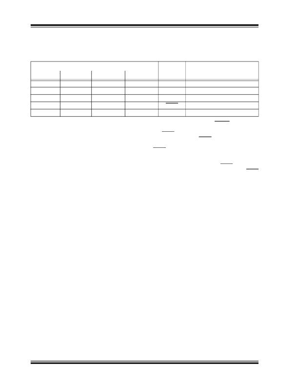
��TABLE� 3-1:�
�MCP1804� PIN� FUNCTION� TABLE�
�MCP1804�
�Symbol�
�Description�
�SOT-23-5�
�SOT-89-5�
�SOT-89-3�
�SOT-223-3�
�1�
�2�
�3�
�4�
�5�
�5�
�2,TAB�
�4�
�3�
�1�
�3�
�2,� TAB�
�—�
�—�
�1�
�3�
�2�
�TAB�
�—�
�1�
�V� IN�
�GND�
�NC�
�SHDN�
�V� OUT�
�Unregulated� Supply� Voltage�
�Ground� Terminal�
�No� connection�
�Shutdown�
�Regulated� Voltage� Output�
�3.1�
�Unregulated� Input� Voltage� (V� IN� )�
�3.3�
�Shutdown� Input� (SHDN)�
�Connect� V� IN� to� the� input� unregulated� source� voltage.�
�Like� all� low� dropout� linear� regulators,� low� source�
�impedance� is� necessary� for� the� stable� operation� of� the�
�LDO.� The� amount� of� capacitance� required� to� ensure�
�low� source� impedance� will� depend� on� the� proximity� of�
�the� input� source� capacitors� or� battery� type.� For� most�
�applications,� 0.1� μF� to� 1.0� μF� of� capacitance� will�
�ensure� stable� operation� of� the� LDO� circuit.� The� type� of�
�capacitor� used� can� be� ceramic,� tantalum� or� aluminum�
�electrolytic.� The� low� ESR� characteristics� of� the� ceramic�
�will� yield� better� noise� and� PSRR� performance� at�
�The� SHDN� input� is� used� to� turn� the� LDO� output� voltage�
�on� and� off.� When� the� SHDN� input� is� at� a� logic-high�
�level,� the� LDO� output� voltage� is� enabled.� When� the�
�SHDN� input� is� pulled� to� a� logic-low� level,� the� LDO�
�output� voltage� is� disabled� and� the� LDO� enters� a� low�
�quiescent� current� shutdown� state� where� the� typical�
�quiescent� current� is� 0.01� μA.� The� SHDN� pin� does� not�
�have� an� internal� pullup� or� pulldown� resistor.� The� SHDN�
�pin� must� be� connected� to� either� V� IN� or� GND� to� prevent�
�the� device� from� becoming� unstable.�
�high-frequency.�
�3.4�
�Regulated� Output� Voltage� (V� OUT� )�
�3.2�
�Ground� Terminal� (GND)�
�Connect� V� OUT� to� the� positive� side� of� the� load� and� the�
�positive� terminal� of� the� output� capacitor.� The� positive�
�Regulator� ground.� Tie� GND� to� the� negative� side� of� the�
�output� and� the� negative� side� of� the� input� capacitor.�
�Only� the� LDO� bias� current� (50� to� 60� μA� typical)� flows�
�out� of� this� pin;� there� is� no� high� current.� The� LDO� output�
�regulation� is� referenced� to� this� pin.� Minimize� voltage�
�drops� between� this� pin� and� the� negative� side� of� the�
�load.�
�DS22200C-page� 16�
�side� of� the� output� capacitor� should� be� physically�
�located� as� close� to� the� LDO� V� OUT� pin� as� is� practical.�
�The� current� flowing� out� of� this� pin� is� equal� to� the� DC�
�load� current.� For� most� applications,� 0.1� μF� to� 1.0� μF� of�
�capacitance� will� ensure� stable� operation� of� the� LDO�
�circuit.� Larger� values� may� be� used� to� improve� dynamic�
�load� response.� The� type� of� capacitor� used� can� be�
�ceramic,� tantalum� or� aluminum� electrolytic.� The� low�
�ESR� characteristics� of� the� ceramic� will� yield� better�
�noise� and� PSRR� performance� at� high-frequency.�
�?� 2011� Microchip� Technology� Inc.�
�相关PDF资料 |
PDF描述 |
|---|---|
| GCC50DRTH | CONN EDGECARD 100PS DIP .100 SLD |
| GSC25DRAN | CONN EDGECARD 50POS R/A .100 SLD |
| RSC26DRAS | CONN EDGECARD 52POS R/A .100 SLD |
| UPM1V271MPD | CAP ALUM 270UF 35V 20% RADIAL |
| RMC26DRAS | CONN EDGECARD 52POS R/A .100 SLD |
相关代理商/技术参数 |
参数描述 |
|---|---|
| MCP1806F600PT-PB | 功能描述:电磁干扰滤波珠子、扼流圈和阵列 1806 60 Ohms TIN/LEAD RoHS:否 制造商:AVX 阻抗: 最大直流电流:35 mA 最大直流电阻: 容差: 端接类型:SMD/SMT 电压额定值:25 V 工作温度范围:- 25 C to + 85 C 封装 / 箱体:0603 (1608 metric) |
| MCP1806F600PT-T | 功能描述:电磁干扰滤波珠子、扼流圈和阵列 1806 Case 60 Ohms RoHS:否 制造商:AVX 阻抗: 最大直流电流:35 mA 最大直流电阻: 容差: 端接类型:SMD/SMT 电压额定值:25 V 工作温度范围:- 25 C to + 85 C 封装 / 箱体:0603 (1608 metric) |
| MCP1806F900PT-PB | 功能描述:电磁干扰滤波珠子、扼流圈和阵列 1806 90 Ohms TIN/LEAD RoHS:否 制造商:AVX 阻抗: 最大直流电流:35 mA 最大直流电阻: 容差: 端接类型:SMD/SMT 电压额定值:25 V 工作温度范围:- 25 C to + 85 C 封装 / 箱体:0603 (1608 metric) |
| MCP1806F900PT-T | 功能描述:电磁干扰滤波珠子、扼流圈和阵列 1806 Case 90 Ohms RoHS:否 制造商:AVX 阻抗: 最大直流电流:35 mA 最大直流电阻: 容差: 端接类型:SMD/SMT 电压额定值:25 V 工作温度范围:- 25 C to + 85 C 封装 / 箱体:0603 (1608 metric) |
| MCP1812F121PT-PB | 功能描述:电磁干扰滤波珠子、扼流圈和阵列 1812 120 Ohms TIN/LEAD RoHS:否 制造商:AVX 阻抗: 最大直流电流:35 mA 最大直流电阻: 容差: 端接类型:SMD/SMT 电压额定值:25 V 工作温度范围:- 25 C to + 85 C 封装 / 箱体:0603 (1608 metric) |
发布紧急采购,3分钟左右您将得到回复。