- 您现在的位置:买卖IC网 > PDF目录13408 > MCP1825S-3302E/AB (Microchip Technology)IC REG LDO 3.3V .5A TO220-3 PDF资料下载
参数资料
| 型号: | MCP1825S-3302E/AB |
| 厂商: | Microchip Technology |
| 文件页数: | 18/38页 |
| 文件大小: | 0K |
| 描述: | IC REG LDO 3.3V .5A TO220-3 |
| 产品培训模块: | High Current LDOs |
| 标准包装: | 50 |
| 稳压器拓扑结构: | 正,固定式 |
| 输出电压: | 3.3V |
| 输入电压: | 最高 6V |
| 电压 - 压降(标准): | 0.21V @ 500mA |
| 稳压器数量: | 1 |
| 电流 - 输出: | 500mA(最小) |
| 工作温度: | -40°C ~ 125°C |
| 安装类型: | 通孔 |
| 封装/外壳: | TO-220-3 |
| 供应商设备封装: | TO-220-3 |
| 包装: | 管件 |
| 产品目录页面: | 666 (CN2011-ZH PDF) |
第1页第2页第3页第4页第5页第6页第7页第8页第9页第10页第11页第12页第13页第14页第15页第16页第17页当前第18页第19页第20页第21页第22页第23页第24页第25页第26页第27页第28页第29页第30页第31页第32页第33页第34页第35页第36页第37页第38页
�� �
�
�MCP1825/MCP1825S�
�4.4�
�Input� Capacitor�
�The� power� good� output� is� an� open-drain� output� that� can�
�Low� input� source� impedance� is� necessary� for� the� LDO�
�output� to� operate� properly.� When� operating� from�
�batteries,� or� in� applications� with� long� lead� length�
�(>� 10� inches)� between� the� input� source� and� the� LDO,�
�some� input� capacitance� is� recommended.� A� minimum�
�of� 1.0� μF� to� 4.7� μF� is� recommended� for� most�
�applications.�
�be� pulled� up� to� any� voltage� that� is� equal� to� or� less� than�
�the� LDO� input� voltage.� This� output� is� capable� of� sinking�
�1.2� mA� (V� PWRGD� <� 0.4V� maximum).�
�VPWRGD_TH�
�For� applications� that� have� output� step� load�
�requirements,� the� input� capacitance� of� the� LDO� is� very�
�important.� The� input� capacitance� provides� the� LDO�
�with� a� good� local� low-impedance� source� to� pull� the�
�transient� currents� from� in� order� to� respond� quickly� to�
�the� output� load� step.� For� good� step� response�
�performance,� the� input� capacitor� should� be� of�
�equivalent� (or� higher)� value� than� the� output� capacitor.�
�The� capacitor� should� be� placed� as� close� to� the� input� of�
�the� LDO� as� is� practical.� Larger� input� capacitors� will� also�
�help� reduce� any� high-frequency� noise� on� the� input� and�
�VOUT�
�PWRGD�
�TPG�
�VOH�
�TVDET_PWRG�
�VOL�
�output� of� the� LDO� and� reduce� the� effects� of� any�
�inductance� that� exists� between� the� input� source�
�voltage� and� the� input� capacitance� of� the� LDO.�
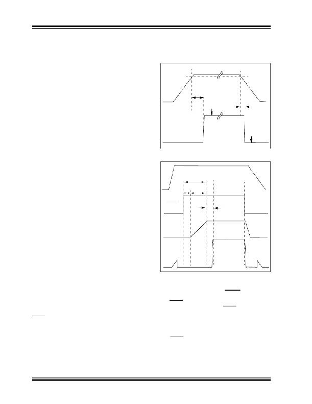
�FIGURE� 4-2:�
�Power� Good� Timing.�
�4.5�
�Power� Good� Output� (PWRGD)�
�V� IN�
�T� OR�
�The� PWRGD� output� is� used� to� indicate� when� the� output�
�voltage� of� the� LDO� is� within� 92%� (typical� value,� see�
��and� Maximum� specifications)� of� its� nominal� regulation�
�value.�
�As� the� output� voltage� of� the� LDO� rises,� the� PWRGD�
�output� will� be� held� low� until� the� output� voltage� has�
�exceeded� the� power� good� threshold� plus� the� hysteresis�
�value.� Once� this� threshold� has� been� exceeded,� the�
�power� good� time� delay� is� started� (shown� as� T� PG� in� the�
�Electrical� Characteristics� table).� The� power� good� time�
�delay� is� fixed� at� 110� μs� (typical).� After� the� time� delay�
�period,� the� PWRGD� output� will� go� high,� indicating� that�
�the� output� voltage� is� stable� and� within� regulation� limits.�
�If� the� output� voltage� of� the� LDO� falls� below� the� power�
�good� threshold,� the� power� good� output� will� transition�
�low.� The� power� good� circuitry� has� a� 170� μs� delay� when�
�detecting� a� falling� output� voltage,� which� helps� to�
�30� μs�
�SHDN�
�V� OUT�
�PWRGD�
�FIGURE� 4-3:�
�Shutdown.�
�70 μ� s�
�T� PG�
�Power� Good� Timing� from�
�increase� noise� immunity� of� the� power� good� output� and�
�avoid� false� triggering� of� the� power� good� output� during�
�4.6�
�Shutdown� Input� (SHDN)�
�fast� output� transients.� See� Figure� 4-2� for� power� good�
�timing� characteristics.�
�When� the� LDO� is� put� into� Shutdown� mode� using� the�
�SHDN� input,� the� power� good� output� is� pulled� low�
�immediately,� indicating� that� the� output� voltage� will� be�
�out� of� regulation.� The� timing� diagram� for� the� power�
�good� output� when� using� the� shutdown� input� is� shown� in�
��DS22056B-page� 18�
�The� SHDN� input� is� an� active-low� input� signal� that� turns�
�the� LDO� on� and� off.� The� SHDN� threshold� is� a�
�percentage� of� the� input� voltage.� The� typical� value� of�
�this� shutdown� threshold� is� 30%� of� V� IN� ,� with� minimum�
�and� maximum� limits� over� the� entire� operating�
�temperature� range� of� 45%� and� 15%,� respectively.�
�The� SHDN� input� will� ignore� low-going� pulses� (pulses�
�meant� to� shut� down� the� LDO)� that� are� up� to� 400� ns� in�
�pulse� width.� If� the� shutdown� input� is� pulled� low� for� more�
�than� 400� ns,� the� LDO� will� enter� Shutdown� mode.� This�
�small� bit� of� filtering� helps� to� reject� any� system� noise�
�spikes� on� the� shutdown� input� signal.�
�?� 2008� Microchip� Technology� Inc.�
�相关PDF资料 |
PDF描述 |
|---|---|
| 10ZLJ4700M12.5X30 | CAP ALUM 4700UF 10V 20% RADIAL |
| MCP1825-3302E/AT | IC REG LDO 3.3V .5A TO220-5 |
| VE-J5P-EX-F3 | CONVERTER MOD DC/DC 13.8V 75W |
| HCM44DRTS | CONN EDGECARD 88POS DIP .156 SLD |
| VE-J5N-EX-F3 | CONVERTER MOD DC/DC 18.5V 75W |
相关代理商/技术参数 |
参数描述 |
|---|---|
| MCP1825S-5002E/AB | 功能描述:低压差稳压器 - LDO 500 mA CMOS LDO Vout 5.0V ETR RoHS:否 制造商:Texas Instruments 最大输入电压:36 V 输出电压:1.4 V to 20.5 V 回动电压(最大值):307 mV 输出电流:1 A 负载调节:0.3 % 输出端数量: 输出类型:Fixed 最大工作温度:+ 125 C 安装风格:SMD/SMT 封装 / 箱体:VQFN-20 |
| MCP1825S-5002E/DB | 功能描述:低压差稳压器 - LDO 500 mA CMOS LDO Vout 5.0V ETR RoHS:否 制造商:Texas Instruments 最大输入电压:36 V 输出电压:1.4 V to 20.5 V 回动电压(最大值):307 mV 输出电流:1 A 负载调节:0.3 % 输出端数量: 输出类型:Fixed 最大工作温度:+ 125 C 安装风格:SMD/SMT 封装 / 箱体:VQFN-20 |
| MCP1825S-5002E/EB | 功能描述:低压差稳压器 - LDO 500 mA CMOS LDO Vout 5.0V ETR RoHS:否 制造商:Texas Instruments 最大输入电压:36 V 输出电压:1.4 V to 20.5 V 回动电压(最大值):307 mV 输出电流:1 A 负载调节:0.3 % 输出端数量: 输出类型:Fixed 最大工作温度:+ 125 C 安装风格:SMD/SMT 封装 / 箱体:VQFN-20 |
| MCP1825ST-0802E/DB | 功能描述:低压差稳压器 - LDO 500 mA CMOS LDO Vout 0.8V ETR RoHS:否 制造商:Texas Instruments 最大输入电压:36 V 输出电压:1.4 V to 20.5 V 回动电压(最大值):307 mV 输出电流:1 A 负载调节:0.3 % 输出端数量: 输出类型:Fixed 最大工作温度:+ 125 C 安装风格:SMD/SMT 封装 / 箱体:VQFN-20 |
| MCP1825ST-0802E/EB | 功能描述:低压差稳压器 - LDO 500 mA CMOS LDO Vout 0.8V ETR RoHS:否 制造商:Texas Instruments 最大输入电压:36 V 输出电压:1.4 V to 20.5 V 回动电压(最大值):307 mV 输出电流:1 A 负载调节:0.3 % 输出端数量: 输出类型:Fixed 最大工作温度:+ 125 C 安装风格:SMD/SMT 封装 / 箱体:VQFN-20 |
发布紧急采购,3分钟左右您将得到回复。