- 您现在的位置:买卖IC网 > PDF目录13386 > MCP1827-2502E/AT (Microchip Technology)IC REG LDO 2.5V 1.5A TO220-5 PDF资料下载
参数资料
| 型号: | MCP1827-2502E/AT |
| 厂商: | Microchip Technology |
| 文件页数: | 19/32页 |
| 文件大小: | 0K |
| 描述: | IC REG LDO 2.5V 1.5A TO220-5 |
| 产品培训模块: | High Current LDOs |
| 标准包装: | 50 |
| 稳压器拓扑结构: | 正,固定式 |
| 输出电压: | 2.5V |
| 输入电压: | 最高 6V |
| 电压 - 压降(标准): | 0.33V @ 1.5A |
| 稳压器数量: | 1 |
| 电流 - 输出: | 1.5A(最小) |
| 工作温度: | -40°C ~ 125°C |
| 安装类型: | 通孔 |
| 封装/外壳: | TO-220-5 |
| 供应商设备封装: | TO-220-5 |
| 包装: | 管件 |
| 产品目录页面: | 667 (CN2011-ZH PDF) |
第1页第2页第3页第4页第5页第6页第7页第8页第9页第10页第11页第12页第13页第14页第15页第16页第17页第18页当前第19页第20页第21页第22页第23页第24页第25页第26页第27页第28页第29页第30页第31页第32页
�� �
�
�MCP1827/MCP1827S�
�5.0�
�5.1�
�APPLICATION�
�CIRCUITS/ISSUES�
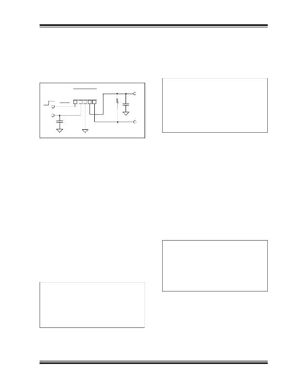
�Typical� Application�
�In� addition� to� the� LDO� pass� element� power� dissipation,�
�there� is� power� dissipation� within� the�
�MCP1827/MCP1827S� as� a� result� of� quiescent� or�
�ground� current.� The� power� dissipation� as� a� result� of� the�
�ground� current� can� be� calculated� using� the� following�
�The� MCP1827/MCP1827S� is� used� for� applications� that�
�require� high� LDO� output� current� and� a� power� good�
�output.�
�V� OUT� =� 2.5V� @� 1.5A�
�equation:�
�EQUATION� 5-2:�
�P� I� (� GND� )� =� V� IN� (� MAX� )� � I� VIN�
�Where:�
�On�
�O� ff�
�3.3V�
�SHDN�
�V� IN�
�C� 1�
�4.7� μF�
�MCP1827-2.5�
�1 2 3 4 5�
�GND�
�R� 1�
�10� k� Ω�
�C� 2�
�10� μF�
�PWRGD�
�P� I(GND�
�V� IN(MAX)�
�I� VIN�
�=�
�=�
�=�
�Power� dissipation� due� to� the�
�quiescent� current� of� the� LDO�
�Maximum� input� voltage�
�Current� flowing� in� the� V� IN� pin�
�with� no� LDO� output� current�
�(LDO� quiescent� current)�
�FIGURE� 5-1:�
�Typical� Application� Circuit.�
�The� total� power� dissipated� within� the�
�MCP1827/MCP1827S� is� the� sum� of� the� power� dissi-�
�5.1.1� APPLICATION� CONDITIONS�
�Package� Type� =� TO-220-5�
�Input� Voltage� Range� =� 3.3V� ±� 5%�
�V� IN� maximum� =� 3.465V�
�V� IN� minimum� =� 3.135V�
�V� DROPOUT� (max)� =� 0.550V�
�V� OUT� (typical)� =� 2.5V�
�I� OUT� =� 1.5A� maximum�
�P� DISS� (typical)� =� 1.2W�
�Temperature� Rise� =� 35.2� °� C�
�pated� in� the� LDO� pass� device� and� the� P(I� GND� )� term.�
�Because� of� the� CMOS� construction,� the� typical� I� GND� for�
�the� MCP1827/MCP1827S� is� 120� μA.� Operating� at� a�
�maximum� of� 3.465V� results� in� a� power� dissipation� of�
�0.49� milli-Watts.� For� most� applications,� this� is� small�
�compared� to� the� LDO� pass� device� power� dissipation�
�and� can� be� neglected.�
�The� maximum� continuous� operating� junction�
�temperature� specified� for� the� MCP1827/MCP1827S� is�
�+125� °� C� .� To� estimate� the� internal� junction� temperature�
�of� the� MCP1827/MCP1827S,� the� total� internal� power�
�dissipation� is� multiplied� by� the� thermal� resistance� from�
�junction� to� ambient� (R� θ� JA� )� of� the� device.� The� thermal�
�resistance� from� junction� to� ambient� for� the� TO-220-5�
�5.2�
�Power� Calculations�
�package� is� estimated� at� 29.3� °� C/W.�
�5.2.1� POWER� DISSIPATION�
�The� internal� power� dissipation� within� the�
�MCP1827/MCP1827S� is� a� function� of� input� voltage,�
�output� voltage,� output� current� and� quiescent� current.�
��power� dissipation� for� the� LDO.�
�EQUATION� 5-1:�
�P� LDO� =� (� V� IN� (� MAX� )� )� –� V� OUT� (� MIN� )� )� ×� I� OUT� (� MAX� )� )�
�Where:�
�EQUATION� 5-3:�
�T� J� (� MAX� )� =� P� TOTAL� ×� R� θ� JA� +� T� AMAX�
�T� J(MAX)� =� Maximum� continuous� junction�
�temperature�
�P� TOTAL� =� Total� device� power� dissipation�
�R� θ� JA� =� Thermal� resistance� from� junction� to�
�ambient�
�T� AMAX� =� Maximum� ambient� temperature�
�P� LDO�
�V� IN(MAX)�
�V� OUT(MIN)�
�=�
�=�
�=�
�LDO� Pass� device� internal�
�power� dissipation�
�Maximum� input� voltage�
�LDO� minimum� output� voltage�
�?� 2007� Microchip� Technology� Inc.�
�DS22001C-page� 19�
�相关PDF资料 |
PDF描述 |
|---|---|
| UPM2A120MED | CAP ALUM 12UF 100V 20% RADIAL |
| 16PX6800MEFCGC16X25 | CAP ALUM 6800UF 16V 20% RADIAL |
| RCB66DHFT-S578 | EDGECARD 132POS .050 SMD W/POSTS |
| UPM2A100MED | CAP ALUM 10UF 100V 20% RADIAL |
| MCP1827-3302E/AT | IC REG LDO 3.3V 1.5A TO220-5 |
相关代理商/技术参数 |
参数描述 |
|---|---|
| MCP1827-3002E/AT | 功能描述:低压差稳压器 - LDO LDO 1.5A CMOS RoHS:否 制造商:Texas Instruments 最大输入电压:36 V 输出电压:1.4 V to 20.5 V 回动电压(最大值):307 mV 输出电流:1 A 负载调节:0.3 % 输出端数量: 输出类型:Fixed 最大工作温度:+ 125 C 安装风格:SMD/SMT 封装 / 箱体:VQFN-20 |
| MCP1827-3002E/AT | 制造商:Microchip Technology Inc 功能描述:IC LDO REG 1.5 A 3 V 5-TO-225 |
| MCP1827-3002E/ET | 功能描述:低压差稳压器 - LDO LDO 1.5A CMOS RoHS:否 制造商:Texas Instruments 最大输入电压:36 V 输出电压:1.4 V to 20.5 V 回动电压(最大值):307 mV 输出电流:1 A 负载调节:0.3 % 输出端数量: 输出类型:Fixed 最大工作温度:+ 125 C 安装风格:SMD/SMT 封装 / 箱体:VQFN-20 |
| MCP1827-3002E/ET | 制造商:Microchip Technology Inc 功能描述:; LEADED PROCESS COMPATIBLE:YES; PEAK RE |
| MCP1827-3302E/AT | 功能描述:低压差稳压器 - LDO LDO 1.5A CMOS RoHS:否 制造商:Texas Instruments 最大输入电压:36 V 输出电压:1.4 V to 20.5 V 回动电压(最大值):307 mV 输出电流:1 A 负载调节:0.3 % 输出端数量: 输出类型:Fixed 最大工作温度:+ 125 C 安装风格:SMD/SMT 封装 / 箱体:VQFN-20 |
发布紧急采购,3分钟左右您将得到回复。