- 您现在的位置:买卖IC网 > PDF目录67986 > MCP23016-I/SP 16 I/O, PIA-GENERAL PURPOSE, PDIP28 PDF资料下载
参数资料
| 型号: | MCP23016-I/SP |
| 元件分类: | 微控制器/微处理器 |
| 英文描述: | 16 I/O, PIA-GENERAL PURPOSE, PDIP28 |
| 封装: | 0.300 INCH, SKINNY, PLASTIC, DIP-28 |
| 文件页数: | 23/38页 |
| 文件大小: | 543K |
| 代理商: | MCP23016-I/SP |
第1页第2页第3页第4页第5页第6页第7页第8页第9页第10页第11页第12页第13页第14页第15页第16页第17页第18页第19页第20页第21页第22页当前第23页第24页第25页第26页第27页第28页第29页第30页第31页第32页第33页第34页第35页第36页第37页第38页
2007 Microchip Technology Inc.
DS20090C-page 3
MCP23016
1.0
DEVICE OVERVIEW
The MCP23016 device provides 16-bit, general
purpose,
parallel
I/O
expansion
for
I2C
bus
applications.
This device includes high-current drive capability, low
supply current and individual I/O configuration. I/O
expanders provide a simple solution when additional
I/Os are needed for ACPI, power switches, sensors,
push buttons, LEDs and so on.
The MCP23016 consists of multiple 8-bit configuration
registers for input, output and polarity selection. The
system master can enable the I/Os as either inputs or
outputs by writing the I/O configuration bits. The data
for each input or output is kept in the corresponding
input or output register. The polarity of the read register
can be inverted with the polarity inversion register (see
“Input
Polarity
Registers”).
All
registers can be read by the system master.
The open-drain interrupt output is activated when any
input state differs from its corresponding input port
register state. This is used to indicate to the system
master that an input state has changed. The interrupt
capture register captures port value at this time. The
Power-on Reset sets the registers to their default val-
ues and initializes the device state machine.
Three device inputs (A0 - A2) determine the I2C
address and allow up to eight I/O expander devices to
share the same I2C bus.
1.1
Pin Descriptions
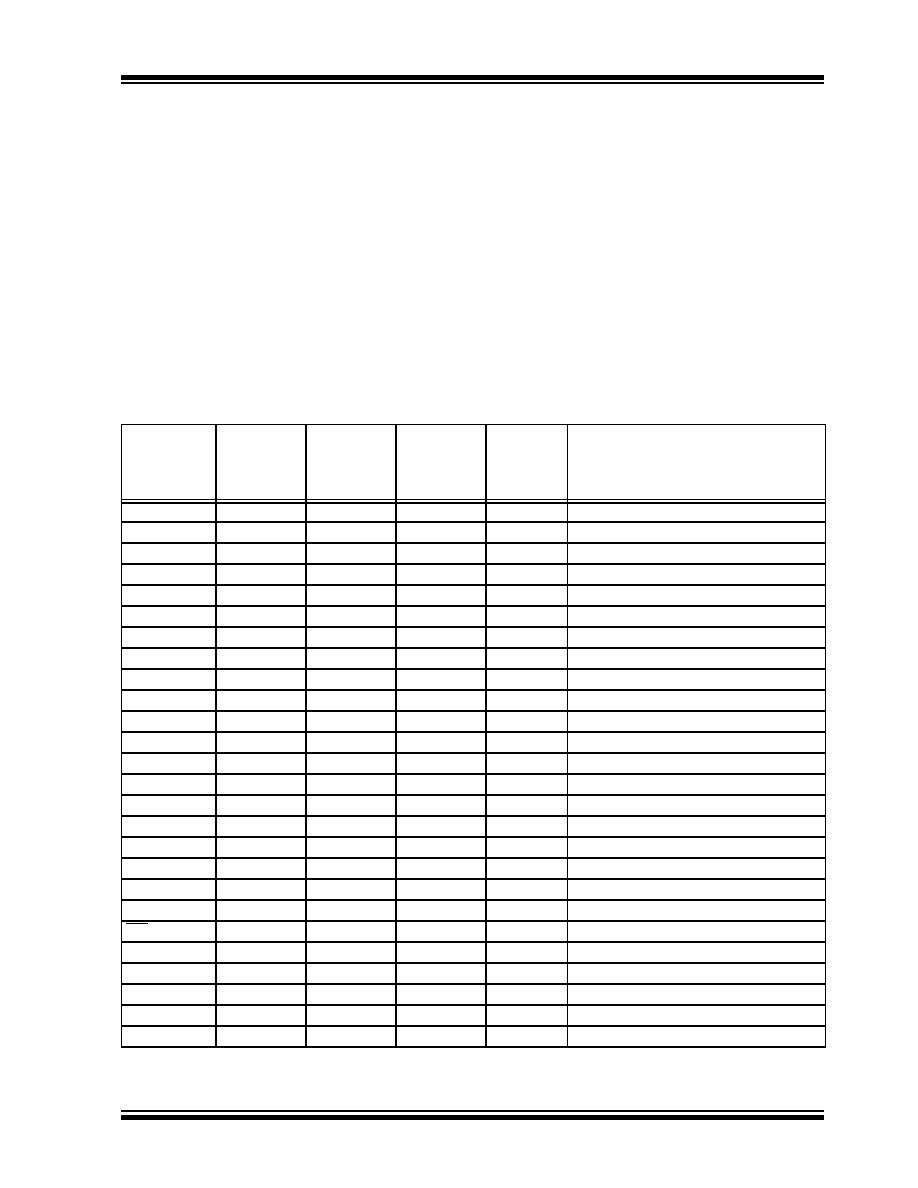
TABLE 1-1:
PINOUT DESCRIPTION
Pin Name
PDIP,
SOIC,
SSOP
Pin No.
QFN
Pin No.
I/O/P
Type
Buffer
Type
Description
CLK
9
6
I
ST
Clock source input
TP
10
7
O
—
Test Pin (This pin must be left floating)
GP1.0
2
27
I/O
TTL
D0 digital input/output for GP1
GP1.1
3
28
I/O
TTL
D1 digital input/output for GP1
GP1.2
4
1
I/O
TTL
D2 digital input/output for GP1
GP1.3
5
2
I/O
TTL
D3 digital input/output for GP1
GP1.4
7
4
I/O
TTL
D4 digital input/output for GP1
GP1.5
11
8
I/O
ST
D5 digital input/output for GP1
GP1.6
12
9
I/O
ST
D6 digital input/output for GP1
GP1.7
13
10
I/O
ST
D7 digital input/output for GP1
GP0.0
21
18
I/O
TTL
D0 digital input/output for GP0
GP0.1
22
19
I/O
TTL
D1 digital input/output for GP0
GP0.2
23
20
I/O
TTL
D2 digital input/output for GP0
GP0.3
24
21
I/O
TTL
D3 digital input/output for GP0
GP0.4
25
22
I/O
TTL
D4 digital input/output for GP0
GP0.5
26
23
I/O
TTL
D5 digital input/output for GP0
GP0.6
27
24
I/O
TTL
D6 digital input/output for GP0
GP0.7
28
25
I/O
TTL
D7 digital input/output for GP0
SCL
14
11
I
ST
Serial clock input
SDA
15
12
I/O
ST
Serial data I/O
INT
6
3
O
OD
Interrupt output
A0
16
13
I
ST
Address input 1
A1
17
14
I
ST
Address input 2
A2
18
15
I
ST
Address input 3
VSS
1, 8, 19
5, 16, 26
P
—
Ground reference for logic and I/O pins
VDD
20
17
P
—
Positive supply for logic and I/O pins
相关PDF资料 |
PDF描述 |
|---|---|
| MCP23S17T-E/SO | 16 I/O, PIA-GENERAL PURPOSE, PDSO28 |
| MCP23017-E/SP | 16 I/O, PIA-GENERAL PURPOSE, PDIP28 |
| MCP23S17-E/SS | 16 I/O, PIA-GENERAL PURPOSE, PDSO28 |
| MCP23S17T-E/ML | 16 I/O, PIA-GENERAL PURPOSE, PQCC28 |
| MCP23017-E/SO | 16 I/O, PIA-GENERAL PURPOSE, PDSO28 |
相关代理商/技术参数 |
参数描述 |
|---|---|
| MCP23016T-I/ML | 功能描述:接口-I/O扩展器 16 bit In/Out RoHS:否 制造商:NXP Semiconductors 逻辑系列: 输入/输出端数量: 最大工作频率:100 kHz 工作电源电压:1.65 V to 5.5 V 工作温度范围:- 40 C to + 85 C 安装风格:SMD/SMT 封装 / 箱体:HVQFN-16 封装:Reel |
| MCP23016T-I/SO | 功能描述:接口-I/O扩展器 16 bit In/Out RoHS:否 制造商:NXP Semiconductors 逻辑系列: 输入/输出端数量: 最大工作频率:100 kHz 工作电源电压:1.65 V to 5.5 V 工作温度范围:- 40 C to + 85 C 安装风格:SMD/SMT 封装 / 箱体:HVQFN-16 封装:Reel |
| MCP23016T-I/SS | 功能描述:接口-I/O扩展器 16 bit In/Out RoHS:否 制造商:NXP Semiconductors 逻辑系列: 输入/输出端数量: 最大工作频率:100 kHz 工作电源电压:1.65 V to 5.5 V 工作温度范围:- 40 C to + 85 C 安装风格:SMD/SMT 封装 / 箱体:HVQFN-16 封装:Reel |
| MCP23017 | 制造商:MICROCHIP 制造商全称:Microchip Technology 功能描述:16-Bit I/O Expander with Serial Interface |
| MCP23017-E/ML | 功能描述:接口-I/O扩展器 16bit Input/Output Exp I2C interface RoHS:否 制造商:NXP Semiconductors 逻辑系列: 输入/输出端数量: 最大工作频率:100 kHz 工作电源电压:1.65 V to 5.5 V 工作温度范围:- 40 C to + 85 C 安装风格:SMD/SMT 封装 / 箱体:HVQFN-16 封装:Reel |
发布紧急采购,3分钟左右您将得到回复。