- 您现在的位置:买卖IC网 > PDF目录10733 > MCP3426A0-E/MC (Microchip Technology)IC ADC 16BIT I2C PROGBL 8-DFN PDF资料下载
参数资料
| 型号: | MCP3426A0-E/MC |
| 厂商: | Microchip Technology |
| 文件页数: | 11/56页 |
| 文件大小: | 0K |
| 描述: | IC ADC 16BIT I2C PROGBL 8-DFN |
| 产品培训模块: | MCP3901 Analog Front End |
| 标准包装: | 150 |
| 位数: | 16 |
| 采样率(每秒): | 15 |
| 数据接口: | I²C,串行 |
| 转换器数目: | 1 |
| 电压电源: | 单电源 |
| 工作温度: | -40°C ~ 125°C |
| 安装类型: | 表面贴装 |
| 封装/外壳: | 8-VFDFN 裸露焊盘 |
| 供应商设备封装: | 8-DFN(2x3) |
| 包装: | 管件 |
| 输入数目和类型: | 2 个差分,单极 |
| 产品目录页面: | 672 (CN2011-ZH PDF) |
第1页第2页第3页第4页第5页第6页第7页第8页第9页第10页当前第11页第12页第13页第14页第15页第16页第17页第18页第19页第20页第21页第22页第23页第24页第25页第26页第27页第28页第29页第30页第31页第32页第33页第34页第35页第36页第37页第38页第39页第40页第41页第42页第43页第44页第45页第46页第47页第48页第49页第50页第51页第52页第53页第54页第55页第56页
2009 Microchip Technology Inc.
DS22226A-page 19
MCP3426/7/8
If the configuration byte is read repeatedly by clocking
continuously after reading the data bytes (i.e., after the
4th byte in the 16-bit conversion mode), the state of the
RDY bit indicates whether the device is ready with new
conversion result. When the Master finds the RDY bit is
cleared, it can send a not-acknowledge (NAK) bit and
a stop bit to exit the current read operation and send a
new read command for the latest conversion data.
Once the conversion data has been read, the ready bit
toggles to ‘1’ until the next new conversion data is
ready. The conversion data in the output register is
overwritten every time a new conversion is completed.
Figure 5-3 shows an example of writing configuration
register, and Figure 5-4 shows an example of reading
conversion data. The user can rewrite the configuration
2 show the examples of the configuration bit operation.
5.3
I2C Serial Communications
The
device
communicates
with
the
Master
(microcontroller) through a serial I2C (Inter-Integrated
Circuit) interface and support standard (100 kbits/sec),
fast (400 kbits/sec) and high-speed (3.4 Mbits/sec)
modes. The serial I2C is a bidirectional 2-wire data bus
communication protocol using open-drain SCL and
SDA lines.
The device can only be addressed as a slave. Once
addressed, it can receive configuration bits with a write
command or transmit the latest conversion results with
a read command. The serial clock pin (SCL) is an input
only and the serial data pin (SDA) is bidirectional. The
Master starts communication by sending a START bit
and terminates the communication by sending a STOP
bit. In read mode, the device releases the SDA line
after receiving NAK and STOP bits.
An example of a hardware connection diagram is
characteristic is described in Section 5.6 “I2C Bus
5.3.1
I2C DEVICE ADDRESSING
The first byte after the START bit is always the address
byte of the device, which includes the device code (4
bits), address bits (3 bits), and R/W bit. The device
code for the devices is 1101, which is programmed at
the factory. The I2C address bits (A2, A1, A0 bits) are
as follows:
MCP3426: Programmed at factory
MCP3427 and MCP3428: Progammed by the
user. It is determined by the logic status of the two
external address selection pins on the user’s
application board (Adr0 and Adr1 pins). The
Master must know the Adr0 and Adr1 pin
conditions before sending read or write command.
and MCP3428)” for more details
Figure 5-1 shows the details of the address byte.
The three I2C address bits allow up to eight devices on
the same I2C bus line. The (R/W) bit determines if the
Master device wants to read the conversion data or
write to the Configuration register. If the (R/W) bit is set
(read mode), the device outputs the conversion data in
the following clocks. If the (R/W) bit is cleared (write
mode), the device expects a configuration byte in the
following clocks. When the device receives the correct
address byte, it outputs an acknowledge bit after the
R/W bit.
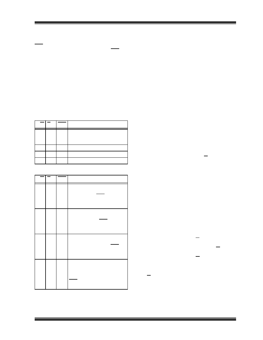
TABLE 5-1:
WRITE CONFIGURATION BITS
R/W O/C
RDY
Operation
00
0
No effect if all other bits remain
the same - operation continues
with the previous settings.
00
1
Initiate One-Shot Conversion.
01
0
Initiate Continuous Conversion.
01
1
Initiate Continuous Conversion.
TABLE 5-2:
READ CONFIGURATION BITS
R/W O/C
RDY
Operation
10
0
New conversion result in One-
Shot conversion mode has just
been read. The RDY bit remains
low until set by a new write
command.
10
1
One-Shot Conversion is in prog-
ress. The conversion result is not
updated yet. The RDY bit stays
high until the current conversion
is completed.
11
0
New conversion result in
Continuous Conversion mode
has just been read. The RDY bit
changes to high after reading the
conversion data.
11
1
The conversion result in
Continuous Conversion mode
was already read. The next new
conversion data is not ready. The
RDY bit stays high until a new
conversion is completed.
相关PDF资料 |
PDF描述 |
|---|---|
| VE-J4X-MY-F3 | CONVERTER MOD DC/DC 5.2V 50W |
| LM2901M | IC COMPARATOR QUAD 14-SOP |
| VE-J4X-MY-F2 | CONVERTER MOD DC/DC 5.2V 50W |
| VI-2WR-MY-B1 | CONVERTER MOD DC/DC 7.5V 50W |
| VE-J4X-MY-F1 | CONVERTER MOD DC/DC 5.2V 50W |
相关代理商/技术参数 |
参数描述 |
|---|---|
| MCP3426A0T-E/MC | 功能描述:模数转换器 - ADC 16-bit delta-sigma ADC dual chan 15sps RoHS:否 制造商:Texas Instruments 通道数量:2 结构:Sigma-Delta 转换速率:125 SPs to 8 KSPs 分辨率:24 bit 输入类型:Differential 信噪比:107 dB 接口类型:SPI 工作电源电压:1.7 V to 3.6 V, 2.7 V to 5.25 V 最大工作温度:+ 85 C 安装风格:SMD/SMT 封装 / 箱体:VQFN-32 |
| MCP3426A0T-E/MS | 功能描述:模数转换器 - ADC 16-bit delta-sigma ADC dual chan 15sps RoHS:否 制造商:Texas Instruments 通道数量:2 结构:Sigma-Delta 转换速率:125 SPs to 8 KSPs 分辨率:24 bit 输入类型:Differential 信噪比:107 dB 接口类型:SPI 工作电源电压:1.7 V to 3.6 V, 2.7 V to 5.25 V 最大工作温度:+ 85 C 安装风格:SMD/SMT 封装 / 箱体:VQFN-32 |
| MCP3426A0T-E/SN | 功能描述:模数转换器 - ADC 16-bit delta-sigma ADC dual chan 15sps RoHS:否 制造商:Texas Instruments 通道数量:2 结构:Sigma-Delta 转换速率:125 SPs to 8 KSPs 分辨率:24 bit 输入类型:Differential 信噪比:107 dB 接口类型:SPI 工作电源电压:1.7 V to 3.6 V, 2.7 V to 5.25 V 最大工作温度:+ 85 C 安装风格:SMD/SMT 封装 / 箱体:VQFN-32 |
| MCP3426A1-E/MC | 功能描述:模数转换器 - ADC 18bit deltasigma ADC single channel, 4sps RoHS:否 制造商:Texas Instruments 通道数量:2 结构:Sigma-Delta 转换速率:125 SPs to 8 KSPs 分辨率:24 bit 输入类型:Differential 信噪比:107 dB 接口类型:SPI 工作电源电压:1.7 V to 3.6 V, 2.7 V to 5.25 V 最大工作温度:+ 85 C 安装风格:SMD/SMT 封装 / 箱体:VQFN-32 |
| MCP3426A1-E/MS | 功能描述:模数转换器 - ADC 18bit deltasigma ADC single channel, 4sps RoHS:否 制造商:Texas Instruments 通道数量:2 结构:Sigma-Delta 转换速率:125 SPs to 8 KSPs 分辨率:24 bit 输入类型:Differential 信噪比:107 dB 接口类型:SPI 工作电源电压:1.7 V to 3.6 V, 2.7 V to 5.25 V 最大工作温度:+ 85 C 安装风格:SMD/SMT 封装 / 箱体:VQFN-32 |
发布紧急采购,3分钟左右您将得到回复。