- 您现在的位置:买卖IC网 > PDF目录10733 > MCP3426A0-E/MC (Microchip Technology)IC ADC 16BIT I2C PROGBL 8-DFN PDF资料下载
参数资料
| 型号: | MCP3426A0-E/MC |
| 厂商: | Microchip Technology |
| 文件页数: | 5/56页 |
| 文件大小: | 0K |
| 描述: | IC ADC 16BIT I2C PROGBL 8-DFN |
| 产品培训模块: | MCP3901 Analog Front End |
| 标准包装: | 150 |
| 位数: | 16 |
| 采样率(每秒): | 15 |
| 数据接口: | I²C,串行 |
| 转换器数目: | 1 |
| 电压电源: | 单电源 |
| 工作温度: | -40°C ~ 125°C |
| 安装类型: | 表面贴装 |
| 封装/外壳: | 8-VFDFN 裸露焊盘 |
| 供应商设备封装: | 8-DFN(2x3) |
| 包装: | 管件 |
| 输入数目和类型: | 2 个差分,单极 |
| 产品目录页面: | 672 (CN2011-ZH PDF) |
第1页第2页第3页第4页当前第5页第6页第7页第8页第9页第10页第11页第12页第13页第14页第15页第16页第17页第18页第19页第20页第21页第22页第23页第24页第25页第26页第27页第28页第29页第30页第31页第32页第33页第34页第35页第36页第37页第38页第39页第40页第41页第42页第43页第44页第45页第46页第47页第48页第49页第50页第51页第52页第53页第54页第55页第56页

2009 Microchip Technology Inc.
DS22226A-page 13
MCP3426/7/8
4.0
DESCRIPTION OF DEVICE
OPERATION
4.1
General Overview
The
MCP3426/7/8
devices
are
differential
multi-channel low-power, 16-Bit Delta-Sigma A/D
converters with an I2C serial interface. The devices
contain an input channel selection multiplexer (mux), a
programmable gain amplifier (PGA), an on-board
voltage reference (2.048V), and an internal oscillator.
When the device powers up (POR is set), it
automatically resets the configuration bits to default
settings.
4.1.1
DEVICE DEFAULT SETTINGS ARE:
Conversion bit resolution: 12 bits (240 sps)
Input channel: Channel 1
PGA gain setting: x1
Continuous conversion
Once the device is powered-up, the user can
reprogram the configuration bits using I2C serial
interface any time. The configuration bits are stored in
the volatile memory.
4.1.2
USER SELECTABLE OPTIONS ARE:
Conversion bit resolution: 12, 14, or 16 bits
Input channel selection: CH1, CH2, CH3, or CH4.
PGA Gain selection: x1, x2, x4, or x8
Continuous or one-shot conversion
In the Continuous Conversion mode, the device
converts the inputs continuously. While in the One-Shot
Conversion mode, the device converts the input one
time and stays in the low-power standby mode until it
receives another command for a new conversion.
During the standby mode, the device consumes less
than 1 A maximum.
4.2
Power-On-Reset (POR)
The device contains an internal Power-On-Reset
(POR) circuit that monitors power supply voltage (VDD)
during operation. This circuit ensures correct device
start-up at system power-up and power-down events.
The device resets all configuration register bits to
default settings as soon as the POR is set.
The POR has built-in hysteresis and a timer to give a
high degree of immunity to potential ripples and noises
on the power supply. A 0.1 F decoupling capacitor
should be mounted as close as possible to the VDD pin
for additional transient immunity.
The threshold voltage is set at 2.2V with a tolerance of
approximately ±5%. If the supply voltage falls below
this threshold, the device will be held in a reset
condition. The typical hysteresis value is approximately
200 mV.
The POR circuit is shut down during the low-power
standby mode. Once a power-up event has occurred,
the
device
requires
additional
delay
time
(approximately 300 s) before a conversion takes
place. During this time, all internal analog circuitries are
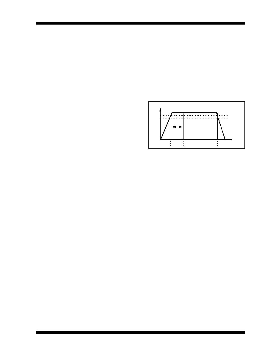
settled before the first conversion occurs. Figure 4-1
illustrates the conditions for power-up and power-down
events under typical start-up conditions.
FIGURE 4-1:
POR Operation.
4.3
Internal Voltage Reference
The device contains an on-board 2.048V voltage
reference. This reference voltage is for internal use
only and not directly measurable. The specification of
the reference voltage is part of the device’s gain and
drift specifications. Therefore, there is no separate
specification for the on-board reference.
4.4
Analog Input Channels
The user can select the input channel using the
configuration register bits. Each channel can be used
for differential or single-ended input.
Each input channel has a switched capacitor input
structure. The internal sampling capacitor (3.2 pF for
PGA = 1) is charged and discharged to process a
conversion. The charging and discharging of the input
sampling capacitor creates dynamic input currents at
each input pin. The current is a function of the
differential input voltages, and inversely proportional to
the internal sampling capacitance, sampling frequency,
and PGA setting.
VDD
2.2V
2.0V
300 S
Reset Start-up
Normal Operation
Reset
Time
相关PDF资料 |
PDF描述 |
|---|---|
| VE-J4X-MY-F3 | CONVERTER MOD DC/DC 5.2V 50W |
| LM2901M | IC COMPARATOR QUAD 14-SOP |
| VE-J4X-MY-F2 | CONVERTER MOD DC/DC 5.2V 50W |
| VI-2WR-MY-B1 | CONVERTER MOD DC/DC 7.5V 50W |
| VE-J4X-MY-F1 | CONVERTER MOD DC/DC 5.2V 50W |
相关代理商/技术参数 |
参数描述 |
|---|---|
| MCP3426A0T-E/MC | 功能描述:模数转换器 - ADC 16-bit delta-sigma ADC dual chan 15sps RoHS:否 制造商:Texas Instruments 通道数量:2 结构:Sigma-Delta 转换速率:125 SPs to 8 KSPs 分辨率:24 bit 输入类型:Differential 信噪比:107 dB 接口类型:SPI 工作电源电压:1.7 V to 3.6 V, 2.7 V to 5.25 V 最大工作温度:+ 85 C 安装风格:SMD/SMT 封装 / 箱体:VQFN-32 |
| MCP3426A0T-E/MS | 功能描述:模数转换器 - ADC 16-bit delta-sigma ADC dual chan 15sps RoHS:否 制造商:Texas Instruments 通道数量:2 结构:Sigma-Delta 转换速率:125 SPs to 8 KSPs 分辨率:24 bit 输入类型:Differential 信噪比:107 dB 接口类型:SPI 工作电源电压:1.7 V to 3.6 V, 2.7 V to 5.25 V 最大工作温度:+ 85 C 安装风格:SMD/SMT 封装 / 箱体:VQFN-32 |
| MCP3426A0T-E/SN | 功能描述:模数转换器 - ADC 16-bit delta-sigma ADC dual chan 15sps RoHS:否 制造商:Texas Instruments 通道数量:2 结构:Sigma-Delta 转换速率:125 SPs to 8 KSPs 分辨率:24 bit 输入类型:Differential 信噪比:107 dB 接口类型:SPI 工作电源电压:1.7 V to 3.6 V, 2.7 V to 5.25 V 最大工作温度:+ 85 C 安装风格:SMD/SMT 封装 / 箱体:VQFN-32 |
| MCP3426A1-E/MC | 功能描述:模数转换器 - ADC 18bit deltasigma ADC single channel, 4sps RoHS:否 制造商:Texas Instruments 通道数量:2 结构:Sigma-Delta 转换速率:125 SPs to 8 KSPs 分辨率:24 bit 输入类型:Differential 信噪比:107 dB 接口类型:SPI 工作电源电压:1.7 V to 3.6 V, 2.7 V to 5.25 V 最大工作温度:+ 85 C 安装风格:SMD/SMT 封装 / 箱体:VQFN-32 |
| MCP3426A1-E/MS | 功能描述:模数转换器 - ADC 18bit deltasigma ADC single channel, 4sps RoHS:否 制造商:Texas Instruments 通道数量:2 结构:Sigma-Delta 转换速率:125 SPs to 8 KSPs 分辨率:24 bit 输入类型:Differential 信噪比:107 dB 接口类型:SPI 工作电源电压:1.7 V to 3.6 V, 2.7 V to 5.25 V 最大工作温度:+ 85 C 安装风格:SMD/SMT 封装 / 箱体:VQFN-32 |
发布紧急采购,3分钟左右您将得到回复。