- 您现在的位置:买卖IC网 > PDF目录5787 > MCP6002T-I/SN (Microchip Technology)IC OPAMP 1.8V 1MHZ DUAL 8-SOIC PDF资料下载
参数资料
| 型号: | MCP6002T-I/SN |
| 厂商: | Microchip Technology |
| 文件页数: | 7/42页 |
| 文件大小: | 0K |
| 描述: | IC OPAMP 1.8V 1MHZ DUAL 8-SOIC |
| 标准包装: | 3,300 |
| 放大器类型: | 通用 |
| 电路数: | 2 |
| 输出类型: | 满摆幅 |
| 转换速率: | 0.6 V/µs |
| 增益带宽积: | 1MHz |
| 电流 - 输入偏压: | 1pA |
| 电压 - 输入偏移: | 4500µV |
| 电流 - 电源: | 100µA |
| 电流 - 输出 / 通道: | 23mA |
| 电压 - 电源,单路/双路(±): | 1.8 V ~ 6 V |
| 工作温度: | -40°C ~ 85°C |
| 安装类型: | 表面贴装 |
| 封装/外壳: | 8-SOIC(0.154",3.90mm 宽) |
| 供应商设备封装: | 8-SOICN |
| 包装: | 带卷 (TR) |
第1页第2页第3页第4页第5页第6页当前第7页第8页第9页第10页第11页第12页第13页第14页第15页第16页第17页第18页第19页第20页第21页第22页第23页第24页第25页第26页第27页第28页第29页第30页第31页第32页第33页第34页第35页第36页第37页第38页第39页第40页第41页第42页
2009 Microchip Technology Inc.
DS21733J-page 15
MCP6001/1R/1U/2/4
FIGURE 4-6:
Example Guard Ring Layout
for Inverting Gain.
1.
Non-inverting Gain and Unity-Gain Buffer:
a.
Connect the non-inverting pin (VIN+) to the
input with a wire that does not touch the
PCB surface.
b.
Connect the guard ring to the inverting input
pin (VIN–). This biases the guard ring to the
common mode input voltage.
2.
Inverting
Gain
and
Transimpedance
Gain
Amplifiers (convert current to voltage, such as
photo detectors):
a.
Connect the guard ring to the non-inverting
input pin (VIN+). This biases the guard ring
to the same reference voltage as the op
amp (e.g., VDD/2 or ground).
b.
Connect the inverting pin (VIN–) to the input
with a wire that does not touch the PCB
surface.
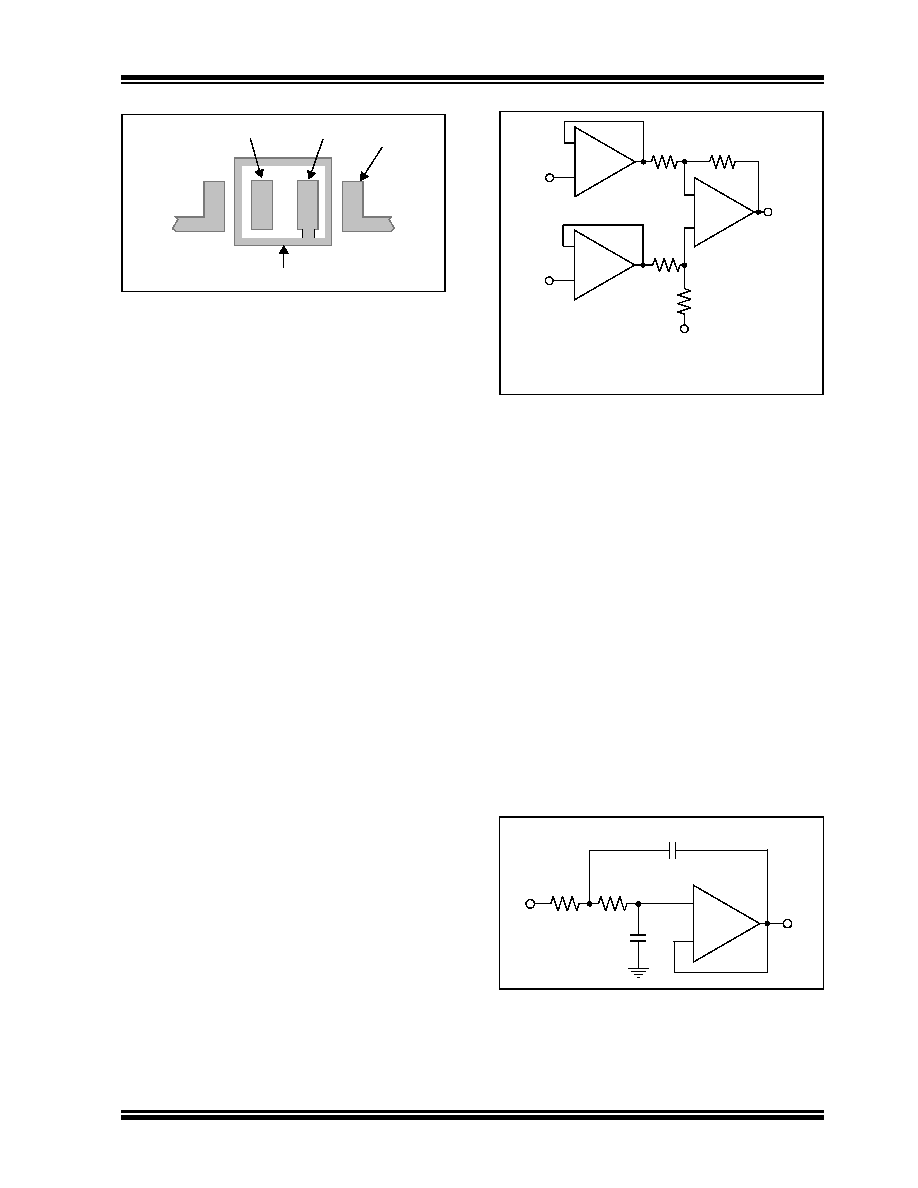
4.7
Application Circuits
4.7.1
UNITY-GAIN BUFFER
The rail-to-rail input and output capability of the
MCP6001/2/4 op amp is ideal for unity-gain buffer
applications. The low quiescent current and wide
bandwidth makes the device suitable for a buffer
configuration in an instrumentation amplifier circuit, as
shown in Figure 4-7.
FIGURE 4-7:
Instrumentation Amplifier
with Unity-Gain Buffer Inputs.
4.7.2
ACTIVE LOW-PASS FILTER
The MCP6001/2/4 op amp’s low input bias current
makes it possible for the designer to use larger
resistors and smaller capacitors for active low-pass
filter
applications.
However,
as
the
resistance
increases,
the
noise
generated
also
increases.
Parasitic capacitances and the large value resistors
could also modify the frequency response. These
trade-offs need to be considered when selecting circuit
elements.
Usually, the op amp bandwidth is 100x the filter cutoff
frequency (or higher) for good performance. It is
possible to have the op amp bandwidth 10X higher
than the cutoff frequency, thus having a design that is
more sensitive to component tolerances.
Figure 4-8 shows a second-order Butterworth filter with
100 kHz cutoff frequency and a gain of +1 V/V; the op
amp bandwidth is only 10x higher than the cutoff
frequency. The component values were selected using
Microchip’s FilterLab software.
FIGURE 4-8:
Active Second-Order
Low-Pass Filter.
Guard Ring
V
SS
VIN-VIN+
VIN1
R2
MCP6002
VIN2
R2
MCP6002
VREF
MCP6001
VOUT
R1
–
+
–
+
–
+
1/2
V
OUT
V
IN2
V
IN1
–
()
R
1
R
2
------
V
REF
+
=
R1 = 20 kΩ
R2 = 10 kΩ
14.3 k
Ω
MCP6002
VOUT
53.6 k
Ω
100 pF
VIN
33 pF
+
–
相关PDF资料 |
PDF描述 |
|---|---|
| LT1469CN8#PBF | IC OPAMP 16BIT DUAL 90MHZ 8DIP |
| 77315-101-08LF | BERGSTIK |
| 75160-118-09LF | BERGSTIK |
| 961128-6404-AR | CONN HEADER VERT SGL 28POS GOLD |
| LT1469CN8 | IC OPAMP 16BIT DUAL 90MHZ 8DIP |
相关代理商/技术参数 |
参数描述 |
|---|---|
| MCP6004 | 制造商:MICROCHIP 制造商全称:Microchip Technology 功能描述:1 MHz, Low-Power Op Amp |
| MCP6004E | 制造商:MICROCHIP 制造商全称:Microchip Technology 功能描述:1 MHz Bandwidth Low Power Op Amp |
| MCP6004-E/LT | 制造商:MICROCHIP 制造商全称:Microchip Technology 功能描述:1 MHz, Low-Power Op Amp |
| MCP6004-E/MS | 制造商:MICROCHIP 制造商全称:Microchip Technology 功能描述:1 MHz, Low-Power Op Amp |
| MCP6004-E/OT | 制造商:MICROCHIP 制造商全称:Microchip Technology 功能描述:1 MHz, Low-Power Op Amp |
发布紧急采购,3分钟左右您将得到回复。