- 您现在的位置:买卖IC网 > PDF目录296503 > MCP604T-E/ST QUAD OP-AMP, 4500 uV OFFSET-MAX, 2.8 MHz BAND WIDTH, PDSO14 PDF资料下载
参数资料
| 型号: | MCP604T-E/ST |
| 元件分类: | 运算放大器 |
| 英文描述: | QUAD OP-AMP, 4500 uV OFFSET-MAX, 2.8 MHz BAND WIDTH, PDSO14 |
| 封装: | 4.40 MM, PLASTIC, MO-153, TSSOP-14 |
| 文件页数: | 3/28页 |
| 文件大小: | 601K |
| 代理商: | MCP604T-E/ST |
第1页第2页当前第3页第4页第5页第6页第7页第8页第9页第10页第11页第12页第13页第14页第15页第16页第17页第18页第19页第20页第21页第22页第23页第24页第25页第26页第27页第28页
2004 Microchip Technology Inc.
DS21314F-page 11
MCP601/2/3/4
3.0
APPLICATIONS INFORMATION
The MCP601/2/3/4 family of op amps are fabricated on
Microchip’s state-of-the-art CMOS process. They are
unity-gain stable and suitable for a wide range of
general purpose applications.
3.1
Input
The MCP601/2/3/4 amplifier family is designed to not
exhibit phase reversal when the input pins exceed the
supply rails. Figure 2-33 shows an input voltage that
exceeds both supplies with no resulting phase
inversion.
The Common Mode Input Voltage Range (VCMR)
includes ground in single-supply systems (VSS), but
does not include VDD. This means that the amplifier
input behaves linearly as long as the Common Mode
Input Voltage (VCM) is kept within the specified VCMR
limits (VSS – 0.3V to VDD – 1.2V at +25°C).
Input voltages that exceed the input voltage range
(VSS – 0.3V to VDD – 1.2V at +25°C) can cause exces-
sive current to flow into or out of the input pins. Current
beyond ±2 mA may cause reliability problems.
Applications that exceed this rating must externally
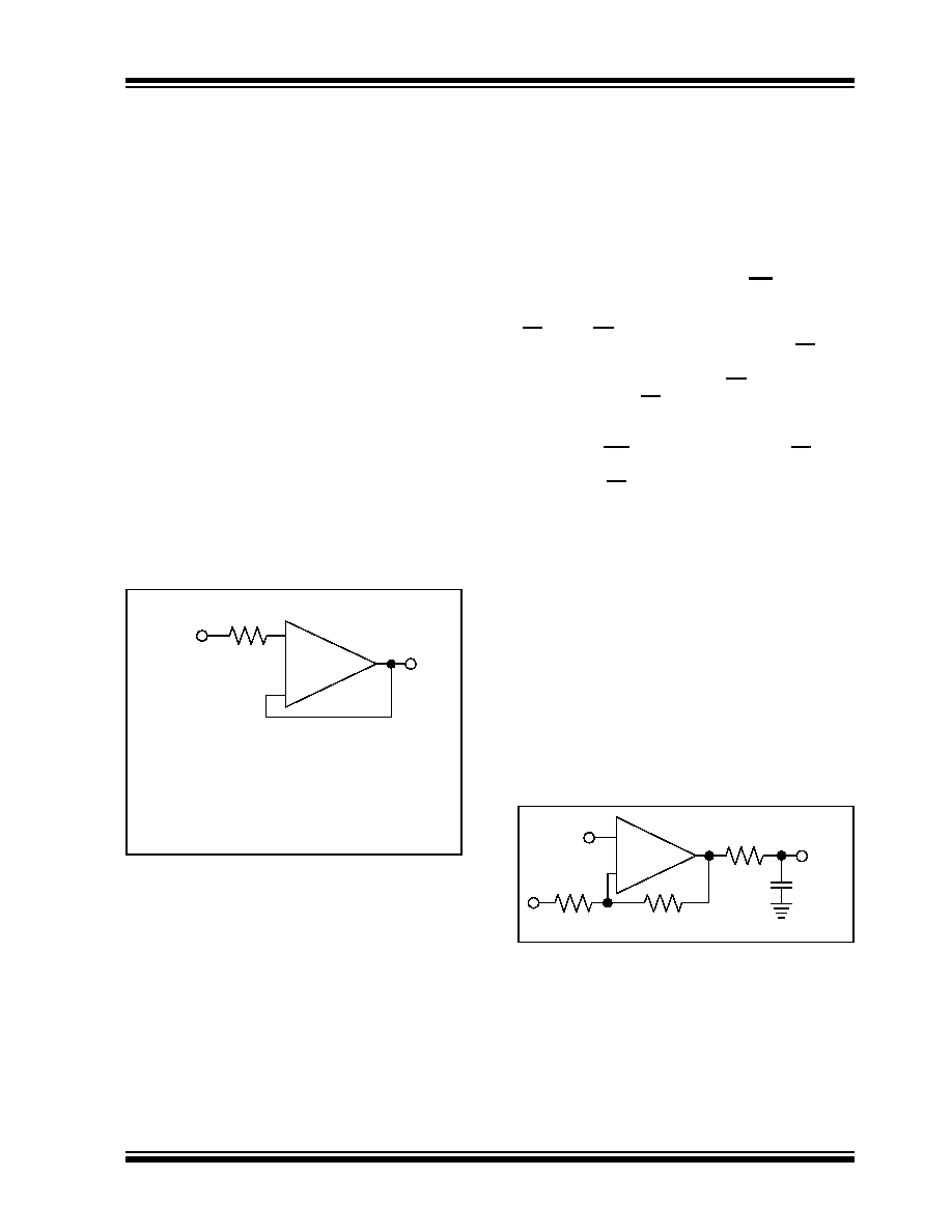
limit the input current with a resistor (RIN), as shown in
FIGURE 3-1:
RIN limits the current flow
into an input pin.
3.2
Rail-to-Rail Output
There are two specifications that describe the output
swing capability of the MCP601/2/3/4 family of op amps.
The first specification (Maximum Output Voltage Swing)
defines the absolute maximum swing that can be
achieved under the specified load conditions. For
instance, the output voltage swings to within 15 mV of
the negative rail with a 25 k
shows how the output voltage is limited when the input
goes beyond the linear region of operation.
The second specification that describes the output
swing capability of these amplifiers is the Linear Output
Voltage Swing. This specification defines the maximum
output swing that can be achieved while the amplifier is
still operating in its linear region. To verify linear
operation in this range, the large signal (DC Open-Loop
Gain (AOL)) is measured at points 100 mV inside the
supply rails. The measurement must exceed the
specified gains in the specification table.
3.3
MCP603 Chip Select (CS)
The MCP603 is a single amplifier with Chip Select
(CS). When CS is pulled high, the supply current drops
to -0.7 A (typ.), which is pulled through the CS pin to
VSS. When this happens, the amplifier output is put into
a high-impedance state. Pulling CS low enables the
amplifier and, if the CS pin is left floating, the amplifier
may not operate properly. Figure 1-1 is the Chip Select
timing diagram and shows the output voltage, supply
currents and CS current in response to a CS pulse.
Figure 2-27 shows the measured output voltage
response to a CS pulse.
3.4
Capacitive Loads
Driving large capacitive loads can cause stability
problems for voltage feedback op amps. As the load
capacitance increases, the feedback loop’s phase
margin decreases and the closed-loop bandwidth is
reduced. This produces gain peaking in the frequency
response with overshoot and ringing in the step
response.
When driving large capacitive loads with these op
amps (e.g., > 40 pF when G = +1), a small series
feedback loop’s phase margin (stability) by making the
output load resistive at higher frequencies. The
bandwidth will be generally lower than the bandwidth
with no capacitive load.
FIGURE 3-2:
Output resistor RISO
stabilizes large capacitive loads.
different capacitive loads and gains. The x-axis is the
normalized load capacitance (CL/GN) in order to make
it easier to interpret the plot for arbitrary gains. GN is the
circuit’s noise gain. For non-inverting gains, GN and the
gain are equal. For inverting gains, GN = 1 + |Gain|
(e.g., -1 V/V gives GN = +2 V/V).
MCP60X
RIN
VIN
+
–
RIN
maximum expected VIN
() VDD
–
2 mA
------------------------------------------------------------------------------
≥
RIN
VSS
minimum expected VIN
()
–
2 mA
---------------------------------------------------------------------------
≥
MCP60X
RISO
VOUT
CL
RF
RG
+
–
相关PDF资料 |
PDF描述 |
|---|---|
| MCP607-I/PG | DUAL OP-AMP, 250 uV OFFSET-MAX, 0.155 MHz BAND WIDTH, PDIP8 |
| MCP607-I/SNG | DUAL OP-AMP, 250 uV OFFSET-MAX, 0.155 MHz BAND WIDTH, PDSO8 |
| MCP6142-E/MS | DUAL OP-AMP, 3000 uV OFFSET-MAX, 0.1 MHz BAND WIDTH, PDSO8 |
| MCP631-E/SN | OP-AMP, 8000 uV OFFSET-MAX, 24 MHz BAND WIDTH, PDSO8 |
| MCP631T-E/SN | OP-AMP, 8000 uV OFFSET-MAX, 24 MHz BAND WIDTH, PDSO8 |
相关代理商/技术参数 |
参数描述 |
|---|---|
| MCP604T-I | 制造商:MICROCHIP 制造商全称:Microchip Technology 功能描述:2.7V to 6.0V Single Supply CMOS Op Amps |
| MCP604T-I/SL | 功能描述:运算放大器 - 运放 Quad 2.7V RoHS:否 制造商:STMicroelectronics 通道数量:4 共模抑制比(最小值):63 dB 输入补偿电压:1 mV 输入偏流(最大值):10 pA 工作电源电压:2.7 V to 5.5 V 安装风格:SMD/SMT 封装 / 箱体:QFN-16 转换速度:0.89 V/us 关闭:No 输出电流:55 mA 最大工作温度:+ 125 C 封装:Reel |
| MCP604T-I/ST | 功能描述:运算放大器 - 运放 Quad 2.7V RoHS:否 制造商:STMicroelectronics 通道数量:4 共模抑制比(最小值):63 dB 输入补偿电压:1 mV 输入偏流(最大值):10 pA 工作电源电压:2.7 V to 5.5 V 安装风格:SMD/SMT 封装 / 箱体:QFN-16 转换速度:0.89 V/us 关闭:No 输出电流:55 mA 最大工作温度:+ 125 C 封装:Reel |
| MCP604T-ICH | 制造商:MICROCHIP 制造商全称:Microchip Technology 功能描述:2.7V to 6.0V Single Supply CMOS Op Amps |
| MCP604T-IOT | 制造商:MICROCHIP 制造商全称:Microchip Technology 功能描述:2.7V to 6.0V Single Supply CMOS Op Amps |
发布紧急采购,3分钟左右您将得到回复。