参数资料
| 型号: | MCP639-E/ML |
| 厂商: | Microchip Technology |
| 文件页数: | 17/62页 |
| 文件大小: | 0K |
| 描述: | IC OP AMP QUAD 24MHZ 16-QFN |
| 标准包装: | 91 |
| 放大器类型: | 通用 |
| 电路数: | 4 |
| 输出类型: | 满摆幅 |
| 转换速率: | 10 V/µs |
| 增益带宽积: | 24MHz |
| 电流 - 输入偏压: | 4pA |
| 电压 - 输入偏移: | 1800µV |
| 电流 - 电源: | 2.5mA |
| 电流 - 输出 / 通道: | 70mA |
| 电压 - 电源,单路/双路(±): | 2.5 V ~ 5.5 V |
| 工作温度: | -40°C ~ 125°C |
| 安装类型: | 表面贴装 |
| 封装/外壳: | 16-VQFN 裸露焊盘 |
| 供应商设备封装: | 16-QFN(4x4) |
| 包装: | 管件 |
第1页第2页第3页第4页第5页第6页第7页第8页第9页第10页第11页第12页第13页第14页第15页第16页当前第17页第18页第19页第20页第21页第22页第23页第24页第25页第26页第27页第28页第29页第30页第31页第32页第33页第34页第35页第36页第37页第38页第39页第40页第41页第42页第43页第44页第45页第46页第47页第48页第49页第50页第51页第52页第53页第54页第55页第56页第57页第58页第59页第60页第61页第62页
MCP631/2/3/4/5/9
DS22197B-page 24
2009-2011 Microchip Technology Inc.
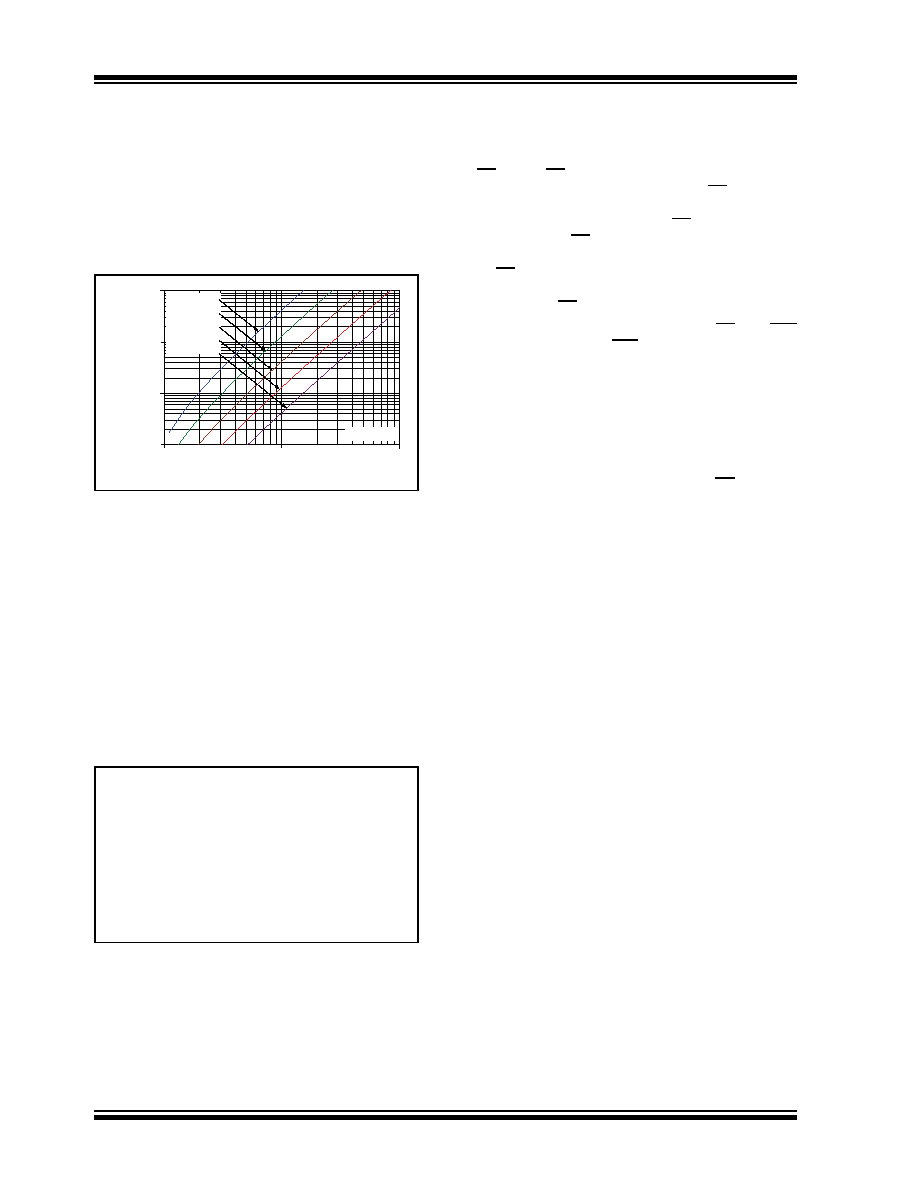
CN and RN form a low-pass filter that affects the signal
at VP. This filter has a single real pole at 1/(2RNCN).
The largest value of RF that should be used depends
several CG values. Some applications may modify
these values to reduce either output loading or gain
peaking (step response overshoot).
FIGURE 4-9:
Maximum Recommended
RF vs. Gain.
Figure 2-34 and Figure 2-35 show the small signal and
large signal step responses at G = +1 V/V. The unity
gain buffer usually has RF =0 and RG open.
Figure 2-36 and Figure 2-37 show the small signal and
large signal step responses at G = -1 V/V. Since the
noise gain is 2 V/V and CG 10 pF, the resistors were
chosen to be RF =RG =1 k and RN = 500.
It is also possible to add a capacitor (CF) in parallel with
RF to compensate for the de-stabilizing effect of CG.
This makes it possible to use larger values of RF. The
conditions for stability are summarized in Equation 4-6.
EQUATION 4-6:
4.4
MCP631, MCP633, MCP635, and
MCP639 Chip Select
The MCP633 is a single amplifier with Chip Select
(CS). When CS is pulled high, the supply current drops
to 1 A (typical) and flows through the CS pin to VSS.
When this happens, the amplifier output is put into a
high-impedance state. By pulling CS low, the amplifier
is enabled. The CS pin has an internal 5 M
(typical)
pull-down resistor connected to VSS, so it will go low if
the CS pin is left floating. Figure 1-1, Figure 2-42 and
Figure 2-43 show the output voltage and supply current
response to a CS pulse.
The MCP635 is a dual amplifier with two CS pins; CSA
controls op amp A and CSB controls op amp B. These
op amps are controlled independently, with an enabled
quiescent current (IQ) of 2.5 mA/amplifier (typical) and
a disabled IQ of 1 A/amplifier (typical). The IQ seen at
the supply pins is the sum of the two op amps’ IQ; the
typical value for the MCP635’s IQ will be 2 A, 2.5 mA
or 5 mA when there are 0, 1 or 2 amplifiers enabled,
respectively.
The MCP639 is a quad amplifier with two CS pins; CSB
controls op amp B and CSD control s op amp D.
4.5
Power Supply
With this family of operational amplifiers, the power
supply pin (VDD for single supply) should have a local
bypass capacitor (i.e., 0.01 F to 0.1 F) within 2 mm
for good high frequency performance. Surface mount,
multilayer ceramic capacitors, or their equivalent,
should be used.
These op amps require a bulk capacitor (i.e., 2.2 F or
larger) within 50 mm to provide large, slow currents.
Tantalum capacitors, or their equivalent, may be a good
choice. This bulk capacitor can be shared with other
nearby analog parts as long as crosstalk through the
supplies does not prove to be a problem.
4.6
High Speed PCB Layout
These op amps are fast enough that a little extra care
in the PCB (Printed Circuit Board) layout can make a
significant difference in performance. Good PC board
layout
techniques
will
help
you
achieve
the
performance shown in the specifications and Typical
Performance Curves; it will also help you minimize
EMC (Electro-Magnetic Compatibility) issues.
Use a solid ground plane. Connect the bypass local
capacitor(s) to this plane with minimal length traces.
This cuts down inductive and capacitive crosstalk.
Separate digital from analog, low speed from high
speed, and low power from high power. This will reduce
interference.
1.E+02
1.E+03
1.E+04
1.E+05
1
10
100
Noise Gain; GN (V/V)
M
ax
im
u
m
R
eco
mme
nd
ed
R
F
(
)
GN > +1 V/V
100
10k
100k
1k
CG = 10 pF
CG = 32 pF
CG = 100 pF
CG = 320 pF
CG = 1 nF
fF fGBWP 2GN2
, GN1 GN2
We need:
GN1
1RF RG
+
=
GN2
1CG CF
+
=
fF
12
R
FCF
=
fZ
fF GN1 GN2
=
Given:
fF fGBWP 4GN1
, GN1 GN2
相关PDF资料 |
PDF描述 |
|---|---|
| MCP6409T-H/SL | IC OPAMP QUAD 1.8V 1MHZ 14SOIC |
| MCP6442-E/MS | IC OPAMP DUAL 1.6V 9KHZ 8MSOP |
| MCP659T-E/ML | IC OP AMP 50MHZ RRIO 16QFN |
| MCP662-E/MS | IC OP AMP 60MHZ DUAL 8-MSOP |
| MCP669T-E/ML | IC OPAMP QUAD 60MHZ 16QFN |
相关代理商/技术参数 |
参数描述 |
|---|---|
| MCP639T-E/ML | 功能描述:运算放大器 - 运放 Quad 24MHz OP w/CS E temp RoHS:否 制造商:STMicroelectronics 通道数量:4 共模抑制比(最小值):63 dB 输入补偿电压:1 mV 输入偏流(最大值):10 pA 工作电源电压:2.7 V to 5.5 V 安装风格:SMD/SMT 封装 / 箱体:QFN-16 转换速度:0.89 V/us 关闭:No 输出电流:55 mA 最大工作温度:+ 125 C 封装:Reel |
| MCP6401RT-E/OT | 功能描述:运算放大器 - 运放 Single 1.8V 1MHz Op E temp RoHS:否 制造商:STMicroelectronics 通道数量:4 共模抑制比(最小值):63 dB 输入补偿电压:1 mV 输入偏流(最大值):10 pA 工作电源电压:2.7 V to 5.5 V 安装风格:SMD/SMT 封装 / 箱体:QFN-16 转换速度:0.89 V/us 关闭:No 输出电流:55 mA 最大工作温度:+ 125 C 封装:Reel |
| MCP6401T-E/LT | 功能描述:运算放大器 - 运放 Single 1.8V 1Mhz Op RoHS:否 制造商:STMicroelectronics 通道数量:4 共模抑制比(最小值):63 dB 输入补偿电压:1 mV 输入偏流(最大值):10 pA 工作电源电压:2.7 V to 5.5 V 安装风格:SMD/SMT 封装 / 箱体:QFN-16 转换速度:0.89 V/us 关闭:No 输出电流:55 mA 最大工作温度:+ 125 C 封装:Reel |
| MCP6401T-E/LT | 制造商:Microchip Technology Inc 功能描述:OPERATIONAL AMPLIFIER (OP-AMP) IC 制造商:Microchip Technology Inc 功能描述:IC, OP-AMP, 1MHZ, 0.5V/ us, SC-70-5 |
| MCP6401T-E/OT | 功能描述:运算放大器 - 运放 Single 1.8V 1Mhz Op RoHS:否 制造商:STMicroelectronics 通道数量:4 共模抑制比(最小值):63 dB 输入补偿电压:1 mV 输入偏流(最大值):10 pA 工作电源电压:2.7 V to 5.5 V 安装风格:SMD/SMT 封装 / 箱体:QFN-16 转换速度:0.89 V/us 关闭:No 输出电流:55 mA 最大工作温度:+ 125 C 封装:Reel |
发布紧急采购,3分钟左右您将得到回复。