- 您现在的位置:买卖IC网 > PDF目录3413 > MCP6H04T-E/ST (Microchip Technology)IC OPAMP QUAD16V 1.2MHZ 14TSSOP PDF资料下载
参数资料
| 型号: | MCP6H04T-E/ST |
| 厂商: | Microchip Technology |
| 文件页数: | 11/46页 |
| 文件大小: | 0K |
| 描述: | IC OPAMP QUAD16V 1.2MHZ 14TSSOP |
| 标准包装: | 2,500 |
| 放大器类型: | 通用 |
| 电路数: | 4 |
| 输出类型: | 满摆幅 |
| 转换速率: | 0.8 V/µs |
| 增益带宽积: | 1.2MHz |
| 电流 - 输入偏压: | 10pA |
| 电压 - 输入偏移: | 700µV |
| 电流 - 电源: | 135µA |
| 电流 - 输出 / 通道: | 50mA |
| 电压 - 电源,单路/双路(±): | 3.5 V ~ 16 V,±1.75 V ~ 8 V |
| 工作温度: | -40°C ~ 125°C |
| 安装类型: | 表面贴装 |
| 封装/外壳: | 14-TSSOP(0.173",4.40mm 宽) |
| 供应商设备封装: | 14-TSSOP |
| 包装: | 带卷 (TR) |
第1页第2页第3页第4页第5页第6页第7页第8页第9页第10页当前第11页第12页第13页第14页第15页第16页第17页第18页第19页第20页第21页第22页第23页第24页第25页第26页第27页第28页第29页第30页第31页第32页第33页第34页第35页第36页第37页第38页第39页第40页第41页第42页第43页第44页第45页第46页
2010-2011 Microchip Technology Inc.
DS22243D-page 19
MCP6H01/2/4
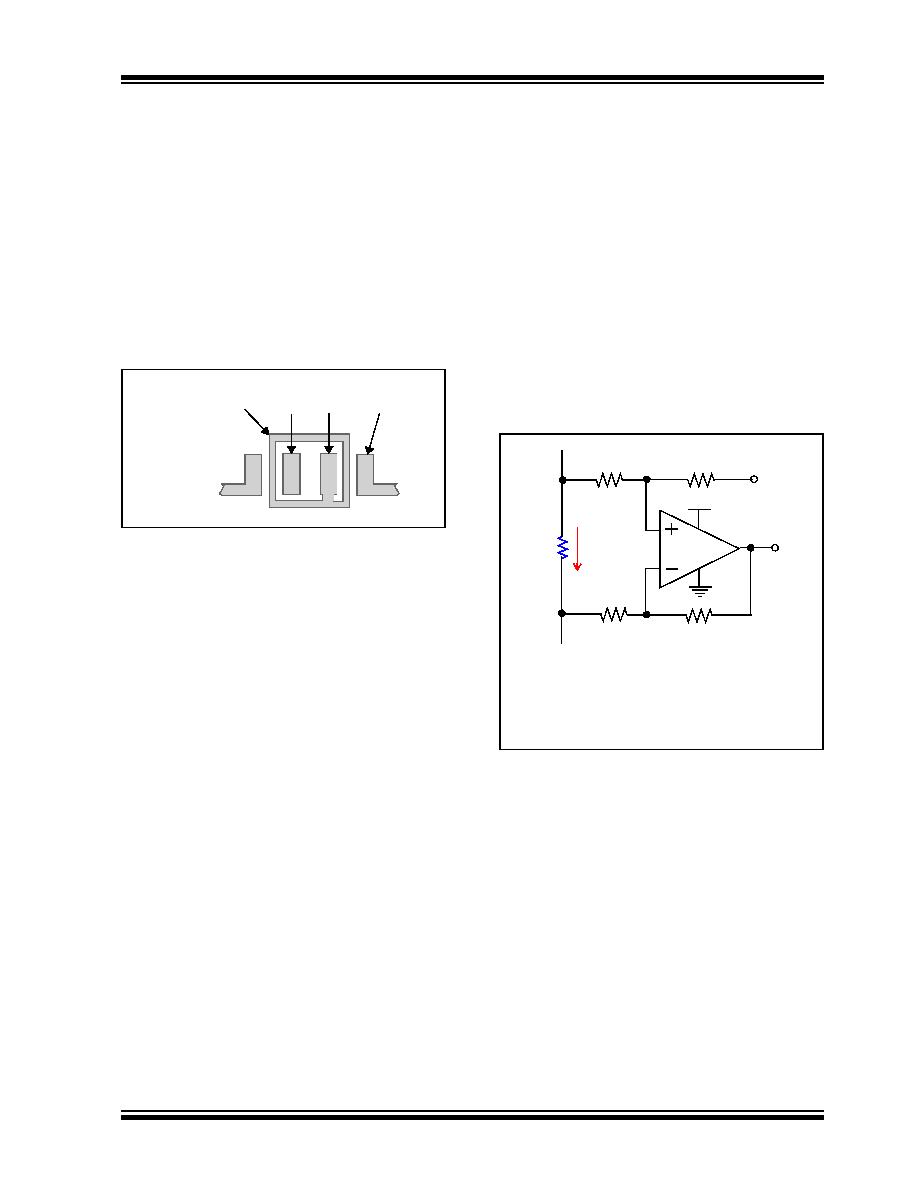
4.6
PCB Surface Leakage
In applications where low input bias current is critical,
PCB surface leakage effects need to be considered.
Surface leakage is caused by humidity, dust or other
contamination on the board. Under low-humidity condi-
tions, a typical resistance between nearby traces is
1012
. A 15V difference would cause 15 pA of current
to flow; which is greater than the MCP6H01/2/4 family’s
bias current at +25°C (10 pA, typical).
The easiest way to reduce surface leakage is to use a
guard ring around sensitive pins (or traces). The guard
ring is biased at the same voltage as the sensitive pin.
An example of this type of layout is shown in
FIGURE 4-7:
Example Guard Ring Layout
for Inverting Gain.
1.
Non-inverting Gain and Unity-Gain Buffer:
a.
Connect the non-inverting pin (VIN+) to the
input with a wire that does not touch the
PCB surface.
b.
Connect the guard ring to the inverting input
pin (VIN–). This biases the guard ring to the
common mode input voltage.
2.
Inverting Gain and Trans-impedance Gain
Amplifiers (convert current to voltage, such as
photo detectors):
a.
Connect the guard ring to the non-inverting
input pin (VIN+). This biases the guard ring
to the same reference voltage as the op
amp (e.g., VDD/2 or ground).
b.
Connect the inverting pin (VIN–) to the input
with a wire that does not touch the PCB
surface.
4.7
Application Circuits
4.7.1
DIFFERENCE AMPLIFIER
The MCP6H01/2/4 op amps can be used in current
sensing applications. Figure 4-8 shows a resistor
(RSEN) that converts the sensor current (ISEN) to
voltage, as well as a difference amplifier that amplifies
the voltage across the resistor while rejecting common
mode noise. R1 and R2 must be well matched to obtain
an
acceptable
Common
Mode
Rejection
Ratio
(CMRR). Moreover, RSEN should be much smaller than
R1 and R2 in order to minimize the resistive loading of
the source.
To ensure proper operation, the op amp common mode
input voltage must be kept within the allowed range.
The reference voltage (VREF) is supplied by a
low-impedance source. In single-supply applications,
VREF is typically VDD/2.
.
FIGURE 4-8:
High Side Current Sensing
Using Difference Amplifier.
Guard Ring
VIN–VIN+
VSS
R1
VOUT
R2
R1
RSEN
ISEN
RSEN << R1, R2
V
OUT
V
1
V
2
–
R
2
R
1
------
V
REF
+
=
VREF
R2
VDD
MCP6H01
相关PDF资料 |
PDF描述 |
|---|---|
| CSR1206FK75L0 | RES .075 OHM 1/2W 1% 1206 SMD |
| 2550-6002UG | CONN HEADER 50POS STR GOLD T/ |
| MCP6293-E/SN | IC OPAMP 2.4V SNGL CS R-R 8SOIC |
| N2516-7003-UB | CONN HEADER 16POS STR GOLD T/H |
| N2516-5003-UB | CONN HEADER 16POS R/A GOLD T/H |
相关代理商/技术参数 |
参数描述 |
|---|---|
| MCP6H71-E/SN | 功能描述:运算放大器 - 运放 16bit deltasigma ADC dual channel 15sps RoHS:否 制造商:STMicroelectronics 通道数量:4 共模抑制比(最小值):63 dB 输入补偿电压:1 mV 输入偏流(最大值):10 pA 工作电源电压:2.7 V to 5.5 V 安装风格:SMD/SMT 封装 / 箱体:QFN-16 转换速度:0.89 V/us 关闭:No 输出电流:55 mA 最大工作温度:+ 125 C 封装:Reel |
| MCP6H71-E/SN | 制造商:Microchip Technology Inc 功能描述:Single 12V 2MHz Opamp 8 SOIC 制造商:Microchip Technology Inc 功能描述:Single, 12V, 2MHz Opamp 8 SOIC 3.90mm(.1 |
| MCP6H71T-E/MNY | 制造商:Microchip Technology Inc 功能描述:SINGLE, 12V, 2MHZ OPAMP - Tape and Reel 制造商:Microchip Technology Inc 功能描述:IC OPAMP GP 2.7MHZ RRO 8TDFN |
| MCP6H71T-E/SN | 制造商:Microchip Technology Inc 功能描述:SINGLE, 12V, 2MHZ OPAMP - Tape and Reel 制造商:Microchip Technology Inc 功能描述:IC OPAMP GP 2.7MHZ RRO 8SOIC |
| MCP6H72-E/SN | 功能描述:运算放大器 - 运放 Single 5MHz OP E tmp RoHS:否 制造商:STMicroelectronics 通道数量:4 共模抑制比(最小值):63 dB 输入补偿电压:1 mV 输入偏流(最大值):10 pA 工作电源电压:2.7 V to 5.5 V 安装风格:SMD/SMT 封装 / 箱体:QFN-16 转换速度:0.89 V/us 关闭:No 输出电流:55 mA 最大工作温度:+ 125 C 封装:Reel |
发布紧急采购,3分钟左右您将得到回复。