- 您现在的位置:买卖IC网 > PDF目录2159 > MCP6V27T-E/SN (Microchip Technology)IC OPAMP DUAL AUTO-ZERO 8SOIC PDF资料下载
参数资料
| 型号: | MCP6V27T-E/SN |
| 厂商: | Microchip Technology |
| 文件页数: | 13/50页 |
| 文件大小: | 0K |
| 描述: | IC OPAMP DUAL AUTO-ZERO 8SOIC |
| 标准包装: | 3,300 |
| 放大器类型: | 自动调零 |
| 电路数: | 2 |
| 输出类型: | 满摆幅 |
| 转换速率: | 1 V/µs |
| 增益带宽积: | 2MHz |
| 电流 - 输入偏压: | 7pA |
| 电压 - 输入偏移: | 2µV |
| 电流 - 电源: | 620µA |
| 电流 - 输出 / 通道: | 22mA |
| 电压 - 电源,单路/双路(±): | 2.3 V ~ 5.5 V |
| 工作温度: | -40°C ~ 125°C |
| 安装类型: | 表面贴装 |
| 封装/外壳: | 8-SOIC(0.154",3.90mm 宽) |
| 供应商设备封装: | 8-SOICN |
| 包装: | 带卷 (TR) |
第1页第2页第3页第4页第5页第6页第7页第8页第9页第10页第11页第12页当前第13页第14页第15页第16页第17页第18页第19页第20页第21页第22页第23页第24页第25页第26页第27页第28页第29页第30页第31页第32页第33页第34页第35页第36页第37页第38页第39页第40页第41页第42页第43页第44页第45页第46页第47页第48页第49页第50页
MCP6V26/7/8
DS25007B-page 20
2011 Microchip Technology Inc.
3.0
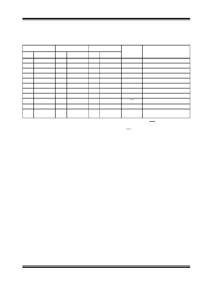
PIN DESCRIPTIONS
Descriptions of the pins are listed in Table 3-1.
TABLE 3-1:
PIN FUNCTION TABLE
3.1
Analog Outputs
The analog output pins (VOUT) are low-impedance
voltage sources.
3.2
Analog Inputs
The non-inverting and inverting inputs (VIN+, VIN–, …)
are high-impedance CMOS inputs with low bias
currents.
3.3
Power Supply Pins
The positive power supply (VDD) is 2.3V to 5.5V higher
than the negative power supply (VSS). For normal
operation, the other pins are between VSS and VDD.
Typically, these parts are used in a single (positive)
supply configuration. In this case, VSS is connected to
ground and VDD is connected to the supply. VDD will
need bypass capacitors.
3.4
Chip Select (CS) Digital Input
This pin (CS) is a CMOS, Schmitt-triggered input that
places the MCP6V28 op amp into a low power mode of
operation.
3.5
Exposed Thermal Pad (EP)
There is an internal connection between the Exposed
Thermal Pad (EP) and the VSS pin; they must be
connected to the same potential on the Printed Circuit
Board (PCB).
This pad can be connected to a PCB ground plane to
provide a larger heat sink. This improves the package
thermal resistance (
θJA).
MCP6V26
MCP6V27
MCP6V28
Symbol
Description
TDFN MSOP, SOIC
DFN
MSOP, SOIC TDFN MSOP, SOIC
66
1
166
VOUT, VOUTA Output (op amp A)
22
2
222
VIN–, VINA– Inverting Input (op amp A)
33
3
333
VIN+, VINA+ Non-inverting Input (op amp A)
44
4
444
VSS
Negative Power Supply
——
5
—
VINB+
Non-inverting Input (op amp B)
——
6
—
VINB–
Inverting Input (op amp B)
——
7
—
VOUTB
Output (op amp B)
77
8
877
VDD
Positive Power Supply
——
—
8
CS
Chip Select (op amp A)
1, 5, 8
—
1, 5
NC
No Internal Connection
9
—
9
—
9
—
EP
Exposed Thermal Pad (EP);
must be connected to VSS
相关PDF资料 |
PDF描述 |
|---|---|
| MCP6V31UT-E/LT | IC OPAMP SGL ZERO DRIFT SC70-5 |
| ME50101VX-000U-A99 | FAN BRUSHLESS 12VDC 50X50X10MM |
| MIC6211BM5 TR | IC OP AMP GEN PURPOSE SOT23-5 |
| MIC7111BM5 TR | IC OPAMP R-R I/O 1.8V SOT23-5 |
| MIC7122BMM | IC OPAMP R-R DUAL 8-MSOP |
相关代理商/技术参数 |
参数描述 |
|---|---|
| MCP6V28-E/MS | 功能描述:运算放大器 - 运放 Sngl, Auto-0 Op Amp w/ Chip Select,E Tmp RoHS:否 制造商:STMicroelectronics 通道数量:4 共模抑制比(最小值):63 dB 输入补偿电压:1 mV 输入偏流(最大值):10 pA 工作电源电压:2.7 V to 5.5 V 安装风格:SMD/SMT 封装 / 箱体:QFN-16 转换速度:0.89 V/us 关闭:No 输出电流:55 mA 最大工作温度:+ 125 C 封装:Reel |
| MCP6V28-E/SN | 功能描述:运算放大器 - 运放 Sngl, Auto-0 Op Amp w/ Chip Select,E Tmp RoHS:否 制造商:STMicroelectronics 通道数量:4 共模抑制比(最小值):63 dB 输入补偿电压:1 mV 输入偏流(最大值):10 pA 工作电源电压:2.7 V to 5.5 V 安装风格:SMD/SMT 封装 / 箱体:QFN-16 转换速度:0.89 V/us 关闭:No 输出电流:55 mA 最大工作温度:+ 125 C 封装:Reel |
| MCP6V28T-E/MNY | 功能描述:运算放大器 - 运放 Sngl, Auto-0 Op Amp w/ Chip Select,E Tmp RoHS:否 制造商:STMicroelectronics 通道数量:4 共模抑制比(最小值):63 dB 输入补偿电压:1 mV 输入偏流(最大值):10 pA 工作电源电压:2.7 V to 5.5 V 安装风格:SMD/SMT 封装 / 箱体:QFN-16 转换速度:0.89 V/us 关闭:No 输出电流:55 mA 最大工作温度:+ 125 C 封装:Reel |
| MCP6V28T-E/MS | 功能描述:运算放大器 - 运放 Sngl, Auto-0 Op Amp w/ Chip Select,E Tmp RoHS:否 制造商:STMicroelectronics 通道数量:4 共模抑制比(最小值):63 dB 输入补偿电压:1 mV 输入偏流(最大值):10 pA 工作电源电压:2.7 V to 5.5 V 安装风格:SMD/SMT 封装 / 箱体:QFN-16 转换速度:0.89 V/us 关闭:No 输出电流:55 mA 最大工作温度:+ 125 C 封装:Reel |
| MCP6V28T-E/SN | 功能描述:运算放大器 - 运放 Sngl, Auto-0 Op Amp w/ Chip Select,E Tmp RoHS:否 制造商:STMicroelectronics 通道数量:4 共模抑制比(最小值):63 dB 输入补偿电压:1 mV 输入偏流(最大值):10 pA 工作电源电压:2.7 V to 5.5 V 安装风格:SMD/SMT 封装 / 箱体:QFN-16 转换速度:0.89 V/us 关闭:No 输出电流:55 mA 最大工作温度:+ 125 C 封装:Reel |
发布紧急采购,3分钟左右您将得到回复。