- 您现在的位置:买卖IC网 > PDF目录19703 > MCZ34653EF (Freescale Semiconductor)IC HOTSWAP CTRLR 1A NEG 8-SOIC PDF资料下载
参数资料
| 型号: | MCZ34653EF |
| 厂商: | Freescale Semiconductor |
| 文件页数: | 15/24页 |
| 文件大小: | 1649K |
| 描述: | IC HOTSWAP CTRLR 1A NEG 8-SOIC |
| 标准包装: | 98 |
| 类型: | 热交换开关 |
| 应用: | 通用 |
| 内部开关: | 是 |
| 电流限制: | 1A |
| 电源电压: | 36 V ~ 80 V |
| 工作温度: | -40°C ~ 85°C |
| 安装类型: | 表面贴装 |
| 封装/外壳: | 8-SOIC(0.154",3.90mm 宽) |
| 供应商设备封装: | 8-SOICN |
| 包装: | 管件 |
Analog Integrated Circuit Device Data
Freescale Semiconductor
15
34653
FUNCTIONAL DEVICE OPERATION
PROTECTION AND DIAGNOSIS FEATURES
rchived by Freescale Semiconductor, Inc., 2008
THERMAL SHUTDOWN
The thermal shutdown feature helps protect the internal
Power MOSFET and circuitry from excessive temperatures.
During start-up and thereafter during normal operation, the
34653 monitors the temperature of the internal circuitry for
excessive heat. If the temperature of the device exceeds the
thermal shutdown temperature of 160癈, one of the start-up
conditions (list on page
10
) is violated, and the device turns
off the Power MOSFET and deactivates the power good
output signals. Until the temperature of the device goes
below 135?/SPAN>C, a new start-up sequence will not be initiated.
This feature is an advantage over solutions with an external
Power MOSFET, because it is not easy for a device with an
external MOSFET to sense the temperature quickly and
accurately. The thermal shutdown circuit is equipped with a
12 約 filter.
Thermal design is critical to proper operation of the 34653.
The typical R
DS(ON)
of the internal Power MOSFET is
0.144 ?at room ambient temperature and can reach up to
0.251 ?at high temperatures. The thermal performance of
the 34653 can vary depending on many factors, among them:
" The ambient operating temperature (T
A
).
" The type of PC board whether it is single layer or multi-
layer, has heat sinks or not, etc. all of which affects the
value of the junction-to-ambient thermal resistance (R
窲A
).
" The value of the desired load current (I
LOAD
).
When choosing an overcurrent limit, certain guidelines
need to be followed to make sure that if the load current is
running close to the overcurrent limit the 34653 does not go
into thermal shutdown. It is good practice to set the
parameters so that the resulting maximum junction
temperature is below the thermal shutdown temperature by a
safe margin.
Equation 1 can be used to calculate the maximum
allowable overcurrent limit based on the maximum desired
junction temperature or vice versa.
The power dissipation in the device can be calculated as
follows:
P = I
2
(LOAD)
*
R
DS(ON)
OR
P = [
T
J
(max) - T
A
(max)] / R
窲A
Combining the two equations:
I
2
(LOAD)
= [
T
J
(max) - T
A
(max)] / [R
窲A
*
R
DS(ON)
] Eq 1
For example:
T
A
(max) = 55癈
R
窲A
= 111 癈/W for a four-layer board
R
DS(ON)
= 0.251 ?at high temperatures
Then:
I
2
(LOAD)
= [
T
J
(max) - 55 癈] / [111 癈/W
*
0.251 ?/SPAN>]
I
2
(LOAD)
= [
T
J
(max) - 55 癈] / 27.86 癈 / A
2
So if the overcurrent limit is 1.0 A, then the maximum
junction temperature is 82.86 癈, which is well below the
thermal shutdown temperature that is allowed.
The previous explanation applies to steady state power
when the device is in normal operation. During the charging
process, the power is dominated by the I * V across the Power
MOSFET. When charging starts, the power in the Power
MOSFET rises up and reaches a maximum value of I * V, then
quickly ramps back down to the steady state level in a period
governed by the size of the loads input capacitor that is being
charged and by the value of the charging current limit I
CHG
.
In this case the instantaneous power dissipation is much
higher than the steady state case, but it is on for a very short
time.
For example:
I
CHG
= 100 mA, the default value
C
LOAD
= 400 ?/SPAN>F, a very large capacitor
V
PWR
= 80 V, worst case
Then:
The power pulse magnitude = I
CHG
*
V
PWR
= 8.0 W
The power pulse duration = C
LOAD *
V
PWR
/ I
CHG
= 320 ms
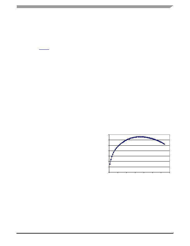
Figure 17
displays the temperature profile of the device
under the instantaneous power pulse during the charging
process. Table 5
depicts thermal resistance values for
different board configurations.
Figure 17. Instantaneous Temperature Rise of an 8.0 W
Power Pulse that Decreases Linearly at End of a
320 ms Period
0.0
10.0
20.0
30.0
40.0
50.0
60.0
70.0
0.000 0.050 0.100 0.150 0.200 0.250 0.300 0.350
Time (sec)
Time (sec)
相关PDF资料 |
PDF描述 |
|---|---|
| CR-2450/H1AN | BATT LITH COIN 3V CELL PC PINS |
| GQM2195C2E8R2CB12D | CAP CER 8.2PF 250V NP0 0805 |
| 183-009-213R171 | CONN DB9 FEMALE .590" R/A NICKEL |
| MCZ34652EF | IC HOTSWAP CTRLR 2A NEG 16SOIC |
| ASC35DRTS | CONN EDGECARD 70POS .100 DIP SLD |
相关代理商/技术参数 |
参数描述 |
|---|---|
| MCZ34653EF/R2 | 制造商:FREESCALE 制造商全称:Freescale Semiconductor, Inc 功能描述:1.0 A Negative Voltage Hot Swap Controller |
| MCZ34653EFR2 | 功能描述:热插拔功率分布 Hot Swap Controller 1.0 Neg Vltg RoHS:否 制造商:Texas Instruments 产品:Controllers & Switches 电流限制: 电源电压-最大:7 V 电源电压-最小:- 0.3 V 工作温度范围: 功率耗散: 安装风格:SMD/SMT 封装 / 箱体:MSOP-8 封装:Tube |
| MCZ34670EG | 功能描述:热插拔功率分布 POWER OVER ETHERNET RoHS:否 制造商:Texas Instruments 产品:Controllers & Switches 电流限制: 电源电压-最大:7 V 电源电压-最小:- 0.3 V 工作温度范围: 功率耗散: 安装风格:SMD/SMT 封装 / 箱体:MSOP-8 封装:Tube |
| MCZ34670EG/R2 | 制造商:FREESCALE 制造商全称:Freescale Semiconductor, Inc 功能描述:IEEE 802.3af PD With Current Mode Switching Regulator |
| MCZ34670EGR2 | 功能描述:热插拔功率分布 POWER OVER ETHERNET RoHS:否 制造商:Texas Instruments 产品:Controllers & Switches 电流限制: 电源电压-最大:7 V 电源电压-最小:- 0.3 V 工作温度范围: 功率耗散: 安装风格:SMD/SMT 封装 / 箱体:MSOP-8 封装:Tube |
发布紧急采购,3分钟左右您将得到回复。