- 您现在的位置:买卖IC网 > PDF目录15503 > MIC2182-5.0YSM (Micrel Inc)IC REG CTRLR BUCK PWM CM 16-SSOP PDF资料下载
参数资料
| 型号: | MIC2182-5.0YSM |
| 厂商: | Micrel Inc |
| 文件页数: | 14/28页 |
| 文件大小: | 0K |
| 描述: | IC REG CTRLR BUCK PWM CM 16-SSOP |
| 标准包装: | 77 |
| PWM 型: | 电流模式 |
| 输出数: | 1 |
| 频率 - 最大: | 330kHz |
| 占空比: | 86% |
| 电源电压: | 4.5 V ~ 32 V |
| 降压: | 是 |
| 升压: | 无 |
| 回扫: | 无 |
| 反相: | 无 |
| 倍增器: | 无 |
| 除法器: | 无 |
| Cuk: | 无 |
| 隔离: | 无 |
| 工作温度: | -40°C ~ 85°C |
| 封装/外壳: | 16-SSOP(0.209",5.30mm 宽) |
| 包装: | 管件 |
| 产品目录页面: | 1092 (CN2011-ZH PDF) |
| 其它名称: | 576-2159 MIC2182-5.0YSM-ND |
第1页第2页第3页第4页第5页第6页第7页第8页第9页第10页第11页第12页第13页当前第14页第15页第16页第17页第18页第19页第20页第21页第22页第23页第24页第25页第26页第27页第28页
�� �
�
�MIC2182�
�The� enable� pin� (pin� 6)� has� two� threshold� levels,� allowing� the�
�MIC2182� to� shut� down� in� a� low� current� mode,� or� turn� off� output�
�switching� in� UVLO� mode.� An� enable� pin� voltage� lower� than�
�the� shutdown� threshold� turns� off� all� the� internal� circuitry� and�
�reduces� the� input� current� to� typically� 0.1� μ� A.�
�If� the� enable� pin� voltage� is� between� the� shutdown� and� UVLO�
�thresholds,� the� internal� bias,� V� DD� ,� and� reference� voltages� are�
�turned� on.� The� soft-start� pin� is� forced� low� by� an� internal�
�discharge� MOSFET.� The� output� drivers� are� inhibited� from�
�switching� and� remain� in� a� low� state.� Raising� the� enable�
�voltage� above� the� UVLO� threshold� of� 2.5V� allows� the� soft-�
�start� capacitor� to� charge� and� enables� the� output� drivers.�
�Either� of� two� UVLO� conditions� will� pull� the� soft-start� capacitor�
�low.�
�?� When� the� V� DD� drops� below� 4.1V�
�?� When� the� enable� pin� drops� below� the� 2.5V�
�threshold�
�MOSFET� Gate� Drive�
�The� MIC2182� high-side� drive� circuit� is� designed� to� switch� an�
�N-channel� MOSFET.� Referring� to� the� block� diagram� in� Figure�
�2,� a� bootstrap� circuit,� consisting� of� D2� and� C� BST� ,� supplies�
�energy� to� the� high-side� drive� circuit.� Capacitor� C� BST� is�
�charged� while� the� low-side� MOSFET� is� on� and� the� voltage� on�
�the� V� SW� pin� (pin� 15)� is� approximately� 0V.� When� the� high-side�
�MOSFET� driver� is� turned� on,� energy� from� C� BST� is� used� to� turn�
�the� MOSFET� on.� As� the� MOSFET� turns� on,� the� voltage� on� the�
�V� SW� pin� increases� to� approximately� V� IN� .� Diode� D2� is� re-�
�versed� biased� and� C� BST� floats� high� while� continuing� to� keep�
�the� high-side� MOSFET� on.� When� the� low-side� switch� is�
�turned� back� on,� C� BST� is� recharged� through� D2.�
�The� drive� voltage� is� derived� from� the� internal� 5V� V� DD� bias�
�supply.� The� nominal� low-side� gate� drive� voltage� is� 5V� and� the�
�nominal� high-side� gate� drive� voltage� is� approximately� 4.5V�
�due� the� voltage� drop� across� D2.� A� fixed� 80ns� delay� between�
�the� high-� and� low-side� driver� transitions� is� used� to� prevent�
�current� from� simultaneously� flowing� unimpeded� through� both�
�MOSFETs.�
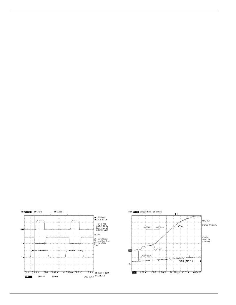
�TIME�
�Figure� 8.� Sync� Waveforms�
�Micrel�
�Oscillator� and� Sync�
�The� internal� oscillator� is� free� running� and� requires� no� external�
�components.� The� nominal� oscillator� frequency� is� 300kHz.� If�
�the� output� voltage� is� below� approximately� 0.95V,� the� oscilla-�
�tor� operates� in� a� frequency-foldback� mode� and� the� switching�
�frequency� is� reduced� to� 60kHz.�
�The� SYNC� input� (pin� 5)� allows� the� MIC2182� to� synchronize�
�with� an� external� clock� signal.� The� rising� edge� of� the� sync�
�signal� generates� a� reset� signal� in� the� oscillator,� which� turns�
�off� the� low-side� gate� drive� output.� The� high-side� drive� then�
�turns� on,� restarting� the� switching� cycle.� The� sync� signal� is�
�inhibited� when� the� controller� operates� in� skip� mode� or� during�
�frequency� foldback.� The� sync� signal� frequency� must� be�
�greater� than� the� maximum� specified� free� running� frequency�
�of� the� MIC2182.� If� the� synchronizing� frequency� is� lower,�
�double� pulsing� of� the� gate� drive� outputs� will� occur.� When� not�
�used,� the� sync� pin� must� be� connected� to� ground.�
�Figure� 8� shows� the� timing� between� the� external� sync� signal�
�(trace� 2),� the� low-side� drive� (trace� 1)� and� the� high-side� drive�
�(trace� R1).� There� is� a� delay� of� approximately� 250ns� between�
�the� rising� edge� of� the� external� sync� signal� and� turnoff� of� the�
�low-side� MOSFET� gate� drive.�
�Some� concerns� of� operating� at� higher� frequencies� are:�
�?� Higher� power� dissipation� in� the� internal� V� DD�
�regulator.� This� occurs� because� the� MOSFET�
�gates� require� charge� to� turn� on� the� device.� The�
�average� current� required� by� the� MOSFET� gate�
�increases� with� switching� frequency.� This� in-�
�creases� the� power� dissipated� by� the� internal�
�V� DD� regulator.� Figure� 10� shows� the� total� gate�
�charge� which� can� be� driven� by� the� MIC2182�
�over� the� input� voltage� range,� for� different� values�
�of� switching� frequency.� The� total� gate� charge�
�includes� both� the� high-� and� low-side� MOSFETs.�
�The� larger� SOP� package� is� capable� of� dissipat-�
�ing� more� power� than� the� SSOP� package� and�
�can� drive� larger� MOSFETs� with� higher� gate�
�drive� requirements.�
�TIME�
�Figure� 9.� Startup� Waveforms�
�M9999-042204�
�14�
�April� 22,� 2004�
�相关PDF资料 |
PDF描述 |
|---|---|
| SPD62-352M | INDUCTOR PWR SHIELDED 3.50UH SMD |
| SPD62-242M | INDUCTOR PWR SHIELDED 2.40UH SMD |
| URZ0J332MHD | CAP ALUM 3300UF 6.3V 20% RADIAL |
| UPM1A122MHD6 | CAP ALUM 1200UF 10V 20% RADIAL |
| UPM2W010MPD | CAP ALUM 1UF 450V 20% RADIAL |
相关代理商/技术参数 |
参数描述 |
|---|---|
| MIC2182BM | 功能描述:IC REG CTRLR BUCK PWM CM 16-SOIC RoHS:否 类别:集成电路 (IC) >> PMIC - 稳压器 - DC DC 切换控制器 系列:- 标准包装:4,000 系列:- PWM 型:电压模式 输出数:1 频率 - 最大:1.5MHz 占空比:66.7% 电源电压:4.75 V ~ 5.25 V 降压:是 升压:无 回扫:无 反相:无 倍增器:无 除法器:无 Cuk:无 隔离:无 工作温度:-40°C ~ 85°C 封装/外壳:40-VFQFN 裸露焊盘 包装:带卷 (TR) |
| MIC2182BM TR | 功能描述:IC REG CTRLR BUCK PWM CM 16-SOIC RoHS:否 类别:集成电路 (IC) >> PMIC - 稳压器 - DC DC 切换控制器 系列:- 标准包装:4,000 系列:- PWM 型:电压模式 输出数:1 频率 - 最大:1.5MHz 占空比:66.7% 电源电压:4.75 V ~ 5.25 V 降压:是 升压:无 回扫:无 反相:无 倍增器:无 除法器:无 Cuk:无 隔离:无 工作温度:-40°C ~ 85°C 封装/外壳:40-VFQFN 裸露焊盘 包装:带卷 (TR) |
| MIC2182BSM | 功能描述:DC/DC 开关控制器 High EfficiencySynchronous Buck Controller SSOP Pkg RoHS:否 制造商:Texas Instruments 输入电压:6 V to 100 V 开关频率: 输出电压:1.215 V to 80 V 输出电流:3.5 A 输出端数量:1 最大工作温度:+ 125 C 安装风格: 封装 / 箱体:CPAK |
| MIC2182BSM TR | 功能描述:DC/DC 开关控制器 High EfficiencySynchronous Buck Controller SSOP Pkg RoHS:否 制造商:Texas Instruments 输入电压:6 V to 100 V 开关频率: 输出电压:1.215 V to 80 V 输出电流:3.5 A 输出端数量:1 最大工作温度:+ 125 C 安装风格: 封装 / 箱体:CPAK |
| MIC2182BSMTR | 制造商:Rochester Electronics LLC 功能描述: 制造商:RF Micro Devices Inc 功能描述: |
发布紧急采购,3分钟左右您将得到回复。