- 您现在的位置:买卖IC网 > PDF目录15503 > MIC2182-5.0YSM (Micrel Inc)IC REG CTRLR BUCK PWM CM 16-SSOP PDF资料下载
参数资料
| 型号: | MIC2182-5.0YSM |
| 厂商: | Micrel Inc |
| 文件页数: | 17/28页 |
| 文件大小: | 0K |
| 描述: | IC REG CTRLR BUCK PWM CM 16-SSOP |
| 标准包装: | 77 |
| PWM 型: | 电流模式 |
| 输出数: | 1 |
| 频率 - 最大: | 330kHz |
| 占空比: | 86% |
| 电源电压: | 4.5 V ~ 32 V |
| 降压: | 是 |
| 升压: | 无 |
| 回扫: | 无 |
| 反相: | 无 |
| 倍增器: | 无 |
| 除法器: | 无 |
| Cuk: | 无 |
| 隔离: | 无 |
| 工作温度: | -40°C ~ 85°C |
| 封装/外壳: | 16-SSOP(0.209",5.30mm 宽) |
| 包装: | 管件 |
| 产品目录页面: | 1092 (CN2011-ZH PDF) |
| 其它名称: | 576-2159 MIC2182-5.0YSM-ND |
第1页第2页第3页第4页第5页第6页第7页第8页第9页第10页第11页第12页第13页第14页第15页第16页当前第17页第18页第19页第20页第21页第22页第23页第24页第25页第26页第27页第28页
�� �
�
�MIC2182�
�Micrel�
�charge� can� be� a� significant� source� of� power� dissipation� in� the�
�MIC2182.� At� low� output� load� this� power� dissipation� is� notice-�
�able� as� a� reduction� in� efficiency.� The� average� current� re-�
�t� T� =�
�C� ISS� � V� GS� +� C� OSS� � V� IN�
�I� G�
�quired� to� drive� the� high-side� MOSFET� is:�
�I� G[high-side](avg)� =� Q� G� � f� S�
�where:�
�I� G[high-side](avg)� =�
�average� high-side� MOSFET� gate� current�
�Q� G� =� total� gate� charge� for� the� high-side� MOSFET�
�taken� from� manufacturer� ’� s� data� sheet�
�with� V� GS� =� 5V.�
�The� low-side� MOSFET� is� turned� on� and� off� at� V� DS� =� 0�
�because� the� freewheeling� diode� is� conducting� during� this�
�time.� The� switching� losses� for� the� low-side� MOSFET� is�
�usually� negligable.� Also,� the� gate� drive� current� for� the� low-�
�side� MOSFET� is� more� accurately� calculated� using� C� ISS� at�
�V� DS� =� 0� instead� of� gate� charge.�
�For� the� low-side� MOSFET:�
�I� G[low-side](avg)� =� C� ISS� � V� GS� � f� S�
�Since� the� current� from� the� gate� drive� comes� from� the� input�
�voltage,� the� power� dissipated� in� the� MIC2182� due� to� gate�
�drive� is:�
�P� gate� drive� =� V� IN� (� I� G[high-side](avg)� +� I� G[low-side](avg)� )�
�A� convenient� figure� of� merit� for� switching� MOSFETs� is� the� on-�
�resistance� times� the� total� gate� charge� (R� DS(on)� � Q� G� ).� Lower�
�numbers� translate� into� higher� efficiency.� Low� gate-charge�
�logic-level� MOSFETs� are� a� good� choice� for� use� with� the�
�MIC2182.� Power� dissipation� in� the� MIC2182� package� limits�
�where:�
�C� ISS� and� C� OSS� are� measured� at� V� DS� =� 0.�
�I� G� =� gate� drive� current� (1A� for� the� MIC2182)�
�The� total� high-side� MOSFET� switching� loss� is:�
�P� AC� =� (V� IN� +� V� D� )� � I� PK� � t� T� � f� S�
�where:�
�t� T� =� switching� transition� time�
�(typically� 20ns� to� 50ns)�
�V� D� =� freewheeling� diode� drop,� typically� 0.5V.�
�f� S� it� the� switching� frequency,� nominally� 300kHz�
�The� low-side� MOSFET� switching� losses� are� negligible� and�
�can� be� ignored� for� these� calculations.�
�RMS� Current� and� MOSFET� Power� Dissipation� Calculation�
�Under� normal� operation,� the� high-side� MOSFET� ’� s� RMS�
�current� is� greatest� when� V� IN� is� low� (maximum� duty� cycle).� The�
�low-side� MOSFET� ’� s� RMS� current� is� greatest� when� V� IN� is� high�
�(minimum� duty� cycle).� However,� the� maximum� stress� the�
�MOSFETs� see� occurs� during� short� circuit� conditions,� where�
�the� output� current� is� equal� to� I� overcurrent(max)� .� (See� the� Sense�
�Resistor� section).� The� calculations� below� are� for� normal�
�operation.� To� calculate� the� stress� under� short� circuit� condi-�
�tions,� substitute� I� overcurrent(max)� for� I� OUT(max)� .� Use� the� formula�
�below� to� calculate� D� under� short� circuit� conditions.�
�D� short� circuit� =� 0.063� ?� 1.8� � 10� ?� 3� � V� IN�
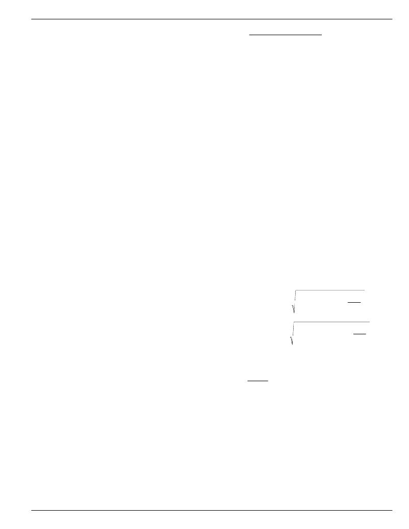
�The� RMS� value� of� the� high-side� switch� current� is:�
�D� � ?� I� OUT(max)2� +� PP� ?�
�the� maximum� gate� drive� current.� Refer� to� Figure� 10� for� the�
�MIC2182� gate� drive� limits.�
�Parameters� that� are� important� to� MOSFET� switch� selection�
�are:�
�I� SW(highside)� (rms)� =�
�?� I� 2� ?�
�?� 12� ?�
�(� 1� ?� D� )� ?� I� OUT(max)2� +�
�?� Voltage� rating�
�?� On-resistance�
�?� Total� gate� charge�
�I� SW(low� side)� (rms)� =�
�?�
�?�
�I� PP2� ?�
�12� ?� ?�
�D� =�
�The� voltage� rating� of� the� MOSFETs� are� essentially� equal� to�
�the� input� voltage.� A� safety� factor� of� 20%� should� be� added� to�
�the� V� DS(max)� of� the� MOSFETs� to� account� for� voltage� spikes�
�due� to� circuit� parasitics.�
�The� power� dissipated� in� the� switching� transistor� is� the� sum� of�
�the� conduction� losses� during� the� on-time� (P� conduction� )� and� the�
�switching� losses� that� occur� during� the� period� of� time� when� the�
�MOSFETs� turn� on� and� off� (P� AC� ).�
�P� SW� =� P� conduction� +� P� AC�
�where:�
�P� conduction� =� I� SW� (rms)� 2� � R� SW�
�P� AC� =� P� AC(off)� +� P� AC(on)�
�where:�
�D� =� duty� cycle� of� the� converter�
�V� OUT�
�η� ×� V� IN�
�η� =� efficiency� of� the� converter.�
�Converter� efficiency� depends� on� component� parameters,�
�which� have� not� yet� been� selected.� For� design� purposes,� an�
�efficiency� of� 90%� can� be� used� for� V� IN� less� than� 10V� and� 85%�
�can� be� used� for� V� IN� greater� than� 10V.� The� efficiency� can� be�
�more� accurately� calculated� once� the� design� is� complete.� If� the�
�assumed� efficiency� is� grossly� inaccurate,� a� second� iteration�
�through� the� design� procedure� can� be� made.�
�For� the� high-side� switch,� the� maximum� dc� power� dissipation�
�R� SW� =� on-resistance� of� the� MOSFET� switch.�
�Making� the� assumption� the� turn-on� and� turnoff� transition�
�times� are� equal,� the� transition� time� can� be� approximated� by:�
�April� 22,� 2004�
�17�
�is:�
�P� switch1(dc)� =� R� DS(on)1� � I� SW1� (rms)� 2�
�M9999-042204�
�相关PDF资料 |
PDF描述 |
|---|---|
| SPD62-352M | INDUCTOR PWR SHIELDED 3.50UH SMD |
| SPD62-242M | INDUCTOR PWR SHIELDED 2.40UH SMD |
| URZ0J332MHD | CAP ALUM 3300UF 6.3V 20% RADIAL |
| UPM1A122MHD6 | CAP ALUM 1200UF 10V 20% RADIAL |
| UPM2W010MPD | CAP ALUM 1UF 450V 20% RADIAL |
相关代理商/技术参数 |
参数描述 |
|---|---|
| MIC2182BM | 功能描述:IC REG CTRLR BUCK PWM CM 16-SOIC RoHS:否 类别:集成电路 (IC) >> PMIC - 稳压器 - DC DC 切换控制器 系列:- 标准包装:4,000 系列:- PWM 型:电压模式 输出数:1 频率 - 最大:1.5MHz 占空比:66.7% 电源电压:4.75 V ~ 5.25 V 降压:是 升压:无 回扫:无 反相:无 倍增器:无 除法器:无 Cuk:无 隔离:无 工作温度:-40°C ~ 85°C 封装/外壳:40-VFQFN 裸露焊盘 包装:带卷 (TR) |
| MIC2182BM TR | 功能描述:IC REG CTRLR BUCK PWM CM 16-SOIC RoHS:否 类别:集成电路 (IC) >> PMIC - 稳压器 - DC DC 切换控制器 系列:- 标准包装:4,000 系列:- PWM 型:电压模式 输出数:1 频率 - 最大:1.5MHz 占空比:66.7% 电源电压:4.75 V ~ 5.25 V 降压:是 升压:无 回扫:无 反相:无 倍增器:无 除法器:无 Cuk:无 隔离:无 工作温度:-40°C ~ 85°C 封装/外壳:40-VFQFN 裸露焊盘 包装:带卷 (TR) |
| MIC2182BSM | 功能描述:DC/DC 开关控制器 High EfficiencySynchronous Buck Controller SSOP Pkg RoHS:否 制造商:Texas Instruments 输入电压:6 V to 100 V 开关频率: 输出电压:1.215 V to 80 V 输出电流:3.5 A 输出端数量:1 最大工作温度:+ 125 C 安装风格: 封装 / 箱体:CPAK |
| MIC2182BSM TR | 功能描述:DC/DC 开关控制器 High EfficiencySynchronous Buck Controller SSOP Pkg RoHS:否 制造商:Texas Instruments 输入电压:6 V to 100 V 开关频率: 输出电压:1.215 V to 80 V 输出电流:3.5 A 输出端数量:1 最大工作温度:+ 125 C 安装风格: 封装 / 箱体:CPAK |
| MIC2182BSMTR | 制造商:Rochester Electronics LLC 功能描述: 制造商:RF Micro Devices Inc 功能描述: |
发布紧急采购,3分钟左右您将得到回复。