- 您现在的位置:买卖IC网 > PDF目录15503 > MIC2184YM (Micrel Inc)IC REG CTRLR BUCK PWM CM 16-SOIC PDF资料下载
参数资料
| 型号: | MIC2184YM |
| 厂商: | Micrel Inc |
| 文件页数: | 9/12页 |
| 文件大小: | 0K |
| 描述: | IC REG CTRLR BUCK PWM CM 16-SOIC |
| 标准包装: | 48 |
| PWM 型: | 电流模式 |
| 输出数: | 1 |
| 频率 - 最大: | 440kHz |
| 占空比: | 100% |
| 电源电压: | 2.9 V ~ 14 V |
| 降压: | 是 |
| 升压: | 无 |
| 回扫: | 无 |
| 反相: | 无 |
| 倍增器: | 无 |
| 除法器: | 无 |
| Cuk: | 无 |
| 隔离: | 无 |
| 工作温度: | -40°C ~ 125°C |
| 封装/外壳: | 16-SOIC(0.154",3.90mm 宽) |
| 包装: | 管件 |
| 产品目录页面: | 1092 (CN2011-ZH PDF) |
| 其它名称: | 576-2161 MIC2184YM-ND |
�� �
�
�MIC2184�
�The� MIC2184� controller� is� broken� down� into� 7� functions.�
�?� Control� loop�
�?� PWM� operation�
�?� Current� mode� control�
�?� Current� limit�
�?� Reference,� enable� and� UVLO�
�?� FreqOut�
�?� MOSFET� gate� drive�
�?� Oscillator� and� Sync�
�?� Soft-start�
�Control� Loop�
�Micrel,� Inc.�
�Current� Limit�
�The� output� current� is� detected� by� the� voltage� drop� across� the�
�external� current� sense� resistor� (R� SENSE� in� Figure� 1.).� The�
�current� sense� resistor� must� be� sized� using� the� minimum�
�current� limit� threshold.� The� external� components� must� be�
�designed� to� withstand� the� maximum� current� limit.� The� current�
�sense� resistor� value� is� calculated� by� the� equation� below:�
�MIN _ CURRENT _ SENSE _ THRESHOLD�
�R� SENSE� =�
�I� OUT� _� MAX�
�The� maximum� output� current� is:�
�PWM� Control� Loop�
�The� MIC2184� uses� current� mode� control� to� regulate� the�
�I� OUT� _� MAX� =�
�MAX _ CURRENT _ SENSE _ THRESHOLD�
�R� SENSE�
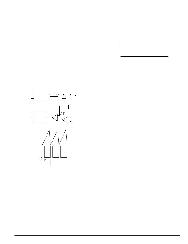
�output� voltage.� This� dual� control� loop� method� (illustrated� in�
�Figure� 2)� senses� the� output� voltage� (outer� loop)� and� the�
�inductor� current� (inner� loop).� It� uses� inductor� current� and�
�output� voltage� to� determine� the� duty� cycle� of� the� buck�
�converter.� Sampling� the� inductor� current� effectively� removes�
�the� inductor� from� the� control� loop,� which� simplifies� compen-�
�sation.�
�V� IN�
�The� current� sense� pins� CSH� (pin� 9)� and� CSL� (pin� 8)� are� noise�
�sensitive� due� to� the� low� signal� level� and� high� input� imped-�
�ance.� The� PCB� traces� should� be� short� and� routed� close� to�
�each� other.� A� small� (1nF)� capacitor� across� the� pins� will�
�attenuate� high� frequency� switching� noise.�
�When� the� peak� inductor� current� exceeds� the� current� limit�
�threshold,� the� overcurrent� comparator� turns� off� the� high� side�
�MOSFET� for� the� remainder� of� the� switching� cycle,� effectively�
�Switching�
�Converter�
�Switch�
�I� INDUCTOR�
�V� OUT�
�Voltage�
�Divider�
�decreasing� the� duty� cycle.� The� output� voltage� drops� as�
�additional� load� current� is� pulled� from� the� converter.� When� the�
�voltage� at� the� feedback� pin� (FB)� reaches� approximately� 0.3V,�
�the� circuit� enters� frequency� foldback� mode� and� the� oscillator�
�frequency� will� drop� to� 1/4� of� the� switching� frequency.� This�
�limits� the� maximum� output� power� delivered� to� the� load� under�
�a� short� circuit� condition.�
�Driver�
�V� ERROR�
�V� REF�
�Reference,� Enable� and� UVLO� Circuits�
�The� output� drivers� are� enabled� when� the� following� conditions�
�I� INDUCTOR�
�V� ERROR�
�t� ON�
�t� PER�
�D� =� t� ON� /t� PER�
�Figure� 2.� Current� Mode� Control� Example�
�As� shown� in� Figure� 1,� the� inductor� current� is� sensed� by�
�measuring� the� voltage� across� the� resistor,� R� SENSE� .� A� ramp� is�
�added� to� the� amplified� current� sense� signal� to� provide� slope�
�compensation,� which� is� required� to� prevent� unstable� opera-�
�tion� at� duty� cycles� greater� than� 50%.�
�A� transconductance� amplifier� is� used� for� the� error� amplifier,�
�which� compares� an� attenuated� sample� of� the� output� voltage�
�with� a� reference� voltage.� The� output� of� the� error� amplifier� is�
�the� compensation� pin� (Comp),� which� is� compared� to� the�
�current� sense� waveform� in� the� PWM� block.� When� the� current�
�signal� becomes� greater� than� the� error� signal,� the� comparator�
�turns� off� the� high� side� drive.� The� COMP� pin� provides� access�
�to� the� output� of� the� error� amplifier� and� allows� the� use� of�
�external� components� to� stabilize� the� voltage� loop.�
�are� satisfied:�
�?� The� V� DD� voltage� (pin� 10)� is� greater� than� its�
�undervoltage� threshold.�
�?� The� voltage� on� the� enable� pin� (pin� 7)� is� greater�
�than� the� enable� UVLO� threshold.�
�The� enable� pin� (pin� 7)� has� two� threshold� levels,� allowing� the�
�MIC2184� to� shut� down� in� a� low� current� mode,� or� turn� off� output�
�switching� in� standby� mode.� An� enable� pin� voltage� lower� than�
�the� shutdown� threshold� turns� off� all� the� internal� circuitry� and�
�places� the� MIC2184� in� a� micropower� shutdown� mode.�
�If� the� enable� pin� voltage� is� between� the� shutdown� and�
�standby� thresholds,� the� internal� bias,� V� DD� and� reference�
�voltages� are� turned� on.� The� soft� start� pin� is� forced� low� by� an�
�internal� discharge� MOSFET.� The� output� drivers� are� inhibited�
�from� switching.� The� OUTP� pin� is� in� a� high� state� and� the� OUTN�
�pin� remains� in� a� low� state.� Raising� the� enable� voltage� above�
�the� standby� threshold� allows� the� soft� start� capacitor� to� charge�
�and� enables� the� output� drivers.� The� standby� threshold� is�
�specified� in� the� electrical� characteristics.� A� resistor� divider�
�can� be� used� with� the� enable� pin� to� prevent� the� power� supply�
�from� turning� on� until� a� specified� input� voltage� is� reached.� The�
�circuit� in� Figure� 3� shows� how� to� connect� the� resistors.�
�April� 2005�
�9�
�M9999-042205�
�相关PDF资料 |
PDF描述 |
|---|---|
| SPD62-472M | INDUCTOR PWR SHIELDED 4.70UH SMD |
| LT3757IDD#PBF | IC REG CTRLR BST FLYBK INV 10DFN |
| MIC2182-5.0YM | IC REG CTRLR BUCK PWM CM 16-SOIC |
| LTC1622IS8#PBF | IC REG CTRLR BUCK PWM CM 8-SOIC |
| MIC2182-5.0YSM | IC REG CTRLR BUCK PWM CM 16-SSOP |
相关代理商/技术参数 |
参数描述 |
|---|---|
| MIC2184YM TR | 功能描述:DC/DC 开关控制器 SO-16 Low Vin Buck PWM Control IC (Lead Free) RoHS:否 制造商:Texas Instruments 输入电压:6 V to 100 V 开关频率: 输出电压:1.215 V to 80 V 输出电流:3.5 A 输出端数量:1 最大工作温度:+ 125 C 安装风格: 封装 / 箱体:CPAK |
| MIC2184YQS | 功能描述:DC/DC 开关控制器 SO-16 Low Vin Synchronous Buck PWM Control IC (Lead Free) RoHS:否 制造商:Texas Instruments 输入电压:6 V to 100 V 开关频率: 输出电压:1.215 V to 80 V 输出电流:3.5 A 输出端数量:1 最大工作温度:+ 125 C 安装风格: 封装 / 箱体:CPAK |
| MIC2184YQS TR | 功能描述:DC/DC 开关控制器 SO-16 Low Vin Synchronous Buck PWM Control IC (Lead Free) RoHS:否 制造商:Texas Instruments 输入电压:6 V to 100 V 开关频率: 输出电压:1.215 V to 80 V 输出电流:3.5 A 输出端数量:1 最大工作温度:+ 125 C 安装风格: 封装 / 箱体:CPAK |
| MIC2185 | 制造商:MICREL 制造商全称:Micrel Semiconductor 功能描述:Low Voltage Synchronous Boost PWM Control IC |
| MIC2185_05 | 制造商:MICREL 制造商全称:Micrel Semiconductor 功能描述:Low Voltage Synchronous Boost PWM Control IC |
发布紧急采购,3分钟左右您将得到回复。