- 您现在的位置:买卖IC网 > PDF目录15114 > MIC2185BQS (Micrel Inc)IC REG CTRLR BST PWM CM 16-QSOP PDF资料下载
参数资料
| 型号: | MIC2185BQS |
| 厂商: | Micrel Inc |
| 文件页数: | 10/15页 |
| 文件大小: | 0K |
| 描述: | IC REG CTRLR BST PWM CM 16-QSOP |
| 标准包装: | 98 |
| PWM 型: | 电流模式 |
| 输出数: | 1 |
| 频率 - 最大: | 440kHz |
| 占空比: | 95% |
| 电源电压: | 2.9 V ~ 14 V |
| 降压: | 无 |
| 升压: | 是 |
| 回扫: | 无 |
| 反相: | 无 |
| 倍增器: | 无 |
| 除法器: | 无 |
| Cuk: | 无 |
| 隔离: | 无 |
| 工作温度: | -40°C ~ 125°C |
| 封装/外壳: | 16-SSOP(0.154",3.90mm 宽) |
| 包装: | 管件 |
�� �
�
�MIC2185�
�Micrel,� Inc.�
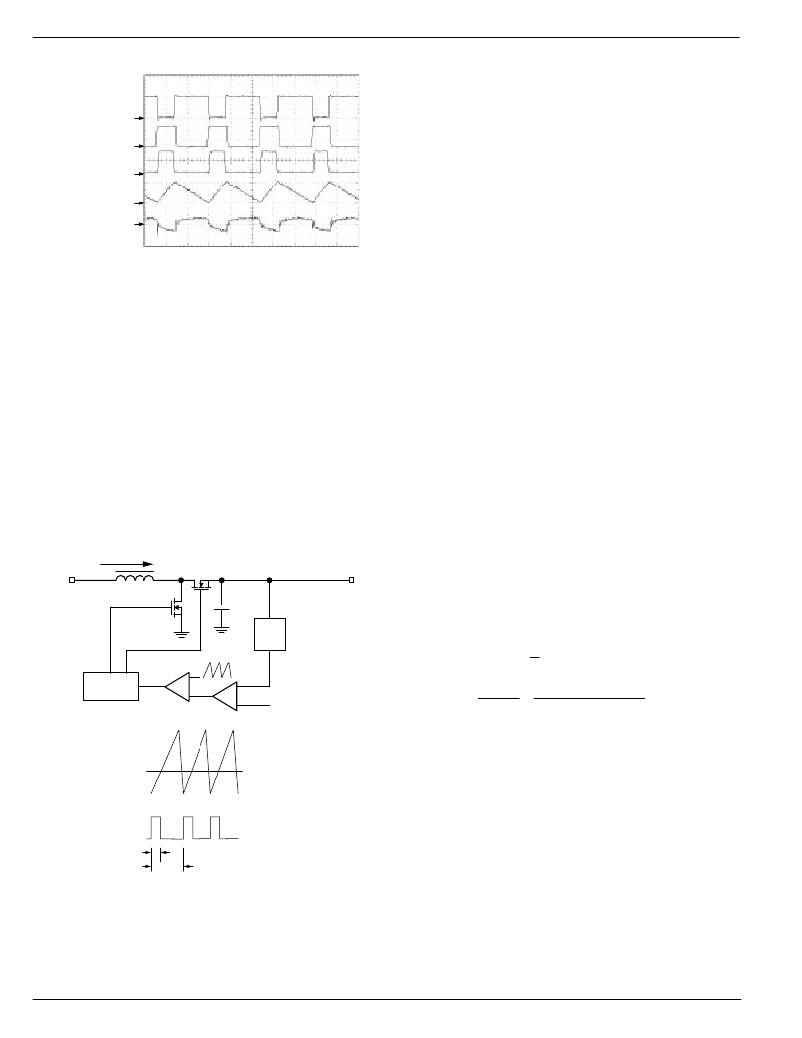
�PWM� Operation�
�Switch� NodeVoltage�
�(Low� Side� FET� Drain)�
�5V/div�
�High� Side� FET�
�Gate� Drive�
�5V/div�
�Low� Side� FET�
�Gate� Drive�
�5V/div�
�Inductor� Current�
�1A� offset;� 0.5A/div�
�V� IN� =� 3.3V�
�PWM� ModeWaveform�
�V� OUT� =� 5V� I� OUT� =� 0.75A�
�required� in� current� mode� control� to� prevent� unstable� operation�
�at� duty� cycles� greater� than� 50%.�
�A� transconductance� ampli?er� is� used� as� an� error� ampli?er,�
�which� compares� an� attenuated� output� voltage� with� a� refer-�
�ence� voltage.� The� output� of� the� error� ampli?er� is� compared�
�to� the� current� sense� waveform� in� the� PWM� block.� When� the�
�current� signal� rises� above� the� error� voltage,� the� comparator�
�turns� off� the� low� side� drive.� The� error� signal� is� brought� out� to�
�the� COMP� pin� (pin� 4)� allowing� the� use� of� external� components�
�to� stabilize� the� voltage� loop.�
�V� OUT� RippleVoltage�
�200mV/div�
�TIME� (1μs/div)�
�Figure� 5� -� PWM� mode� waveforms�
�Figure� 5� shows� typical� waveforms� for� PWM� mode� of� operation.�
�The� gate� drive� signal� turns� on� the� external� low� side� MOSFET,�
�Q1,� allowing� the� inductor� current� to� ramp� up.� When� the� low�
�side� MOSFET� turns� off� and� the� high� side� MOSFET,� Q2,� turns�
�on,� current� ?owing� in� the� inductor� forces� the� MOSFET� drain�
�voltage� to� rise� until� the� is� clamped� at� approximately� the� output�
�voltage.� The� MIC2185� uses� current� mode� control� to� improve�
�output� regulation� and� simplify� compensation� of� the� control�
�loop.� Current� mode� control� senses� both� the� output� voltage�
�(outer� loop)� and� the� inductor� current� (inner� loop).� It� uses� the�
�inductor� current� and� output� voltage� to� determine� the� duty�
�cycle� (D)� of� the� buck� converter.� Sampling� the� inductor� current�
�effectively� removes� the� inductor� from� the� control� loop,� which�
�simpli?es� compensation.� A� simpli?ed� current� mode� control�
�diagram� is� shown� in� ?gure� 6.�
�I_inductor�
�V� IN�
�Current� Sensing� and� Overcurrent� Protection�
�The� inductor� current� is� sensed� during� the� switch� on� time� by�
�a� current� sense� resistor� located� between� the� source� of� the�
�MOSFET,� Q1� and� ground� (R� SENSE� in� Figure� 1).� Exceeding�
�the� current� limit� threshold� will� immediately� terminate� the�
�gate� drive� of� the� N-channel� MOSFET.� This� forces� the� Q1� to�
�operate� at� a� reduced� duty� cycle,� which� reduces� the� output�
�voltage.� In� a� boost� converter,� the� overcurrent� limit� will�
�not� protect� the� power� supply� or� load� during� a� severe�
�overcurrent� condition� or� short� circuit� condition.� If� the�
�output� is� short-circuited� to� ground,� current� will� ?ow� from� the�
�input,� through� the� inductor� and� output� diode,D1,� to� ground.�
�Only� the� impedance� of� the� source� and� components� limits�
�the� current.�
�The� minimum� input� voltage,� maximum� output� power� and�
�the� minimum� value� of� the� current� limit� threshold� determine�
�the� value� of� the� current� sense� resistor.� The� two� switch,� syn-�
�chronous� operation� of� the� MIC2185� forces� the� converter� to�
�always� operate� in� the� continuous� mode� because� current� can�
�?ow� both� ways� through� the� high� side� P-channel� MOSFET.�
�The� equations� below� will� help� to� determine� the� current� sense�
�resistor� value.�
�Maximum� Peak� Current�
�The� peak� inductor� current� is� equal� to� the� average� inductor�
�current� plus� one� half� of� the� peak� to� peak� inductor� current.�
�I� IND(pk)� =� I� IND(ave)� +�
�� I� IND(pp)�
�V� O� ×� I� O� V� L� ×� (� V� O� ?� (� V� IN� ×� η� )� )�
�V� IN� ×� η�
�2� � V� O� � fs� � L�
�Gate� Driver�
�V� COMP�
�I_inductor�
�I_inductor�
�I_inductor�
�Voltage�
�Divider�
�V� REF�
�The� peak� inductor� current� is:�
�1�
�2�
�I� IND(pk)� =� +�
�where:�
�I� O� is� the� maximum� output� current�
�V� O� is� the� output� voltage�
�V� IN� is� the� minimum� input� voltage�
�L� is� the� value� of� the� boost� inductor�
�T� ON�
�Gate� Drive� at� OUTN�
�f� S� is� the� switching� frequency�
�η� is� the� ef?ciency� of� the� boost� converter�
�T� PER�
�Figure� 6.� PWM� Control� Loop�
�A� block� diagram� of� the� MIC2185� PWM� current� mode� control�
�loop� is� shown� in� Figure� 1.� The� inductor� current� is� sensed� by�
�measuring� the� voltage� across� a� resistor,� Rsense.� The� current�
�sense� ampli?er� buffers� and� ampli?es� this� signal.� A� ramp� is�
�added� to� this� signal� to� provide� slope� compensation,� which� is�
�V� L� is� the� voltage� across� the� inductor�
�V� L� may� be� approximated� as� V� IN� for� higher� input� voltage.�
�However,� the� voltage� drop� across� the� inductor� winding�
�resistance� and� low� side� MOSFET� on-resistance� must� be�
�accounted� for� at� the� lower� input� voltages� that� the� MIC2185�
�can� operate� at:�
�MIC2185�
�10�
�October� 2005�
�相关PDF资料 |
PDF描述 |
|---|---|
| GCM44DRPH | CONN EDGECARD 88POS DIP .156 SLD |
| SLPX393M010H3P3 | CAP ALUM 39000UF 10V 20% SNAP |
| VE-21Z-EX-B1 | CONVERTER MOD DC/DC 2V 30W |
| UPM1J102MHD | CAP ALUM 1000UF 63V 20% RADIAL |
| RCC26DRYS-S93 | CONN EDGECARD 52POS DIP .100 SLD |
相关代理商/技术参数 |
参数描述 |
|---|---|
| MIC2185BQS TR | 功能描述:IC REG CTRLR BST PWM CM 16-QSOP RoHS:否 类别:集成电路 (IC) >> PMIC - 稳压器 - DC DC 切换控制器 系列:- 标准包装:4,000 系列:- PWM 型:电压模式 输出数:1 频率 - 最大:1.5MHz 占空比:66.7% 电源电压:4.75 V ~ 5.25 V 降压:是 升压:无 回扫:无 反相:无 倍增器:无 除法器:无 Cuk:无 隔离:无 工作温度:-40°C ~ 85°C 封装/外壳:40-VFQFN 裸露焊盘 包装:带卷 (TR) |
| MIC2185YM | 功能描述:DC/DC 开关控制器 SO-16 Low Vin Synchronous Buck PWM Control IC (Lead Free) RoHS:否 制造商:Texas Instruments 输入电压:6 V to 100 V 开关频率: 输出电压:1.215 V to 80 V 输出电流:3.5 A 输出端数量:1 最大工作温度:+ 125 C 安装风格: 封装 / 箱体:CPAK |
| MIC2185YM TR | 功能描述:DC/DC 开关控制器 SO-16 Low Vin Synchronous Buck PWM Control IC (Lead Free) RoHS:否 制造商:Texas Instruments 输入电压:6 V to 100 V 开关频率: 输出电压:1.215 V to 80 V 输出电流:3.5 A 输出端数量:1 最大工作温度:+ 125 C 安装风格: 封装 / 箱体:CPAK |
| MIC2185YQS | 功能描述:DC/DC 开关控制器 SO-16 Low Vin Synchronous Buck PWM Control IC (Lead Free) RoHS:否 制造商:Texas Instruments 输入电压:6 V to 100 V 开关频率: 输出电压:1.215 V to 80 V 输出电流:3.5 A 输出端数量:1 最大工作温度:+ 125 C 安装风格: 封装 / 箱体:CPAK |
| MIC2185YQS TR | 功能描述:DC/DC 开关控制器 SO-16 Low Vin Synchronous Buck PWM Control IC (Lead Free) RoHS:否 制造商:Texas Instruments 输入电压:6 V to 100 V 开关频率: 输出电压:1.215 V to 80 V 输出电流:3.5 A 输出端数量:1 最大工作温度:+ 125 C 安装风格: 封装 / 箱体:CPAK |
发布紧急采购,3分钟左右您将得到回复。