- 您现在的位置:买卖IC网 > PDF目录15503 > MIC2185YM (Micrel Inc)IC REG CTRLR BST PWM CM 16-SOIC PDF资料下载
参数资料
| 型号: | MIC2185YM |
| 厂商: | Micrel Inc |
| 文件页数: | 11/15页 |
| 文件大小: | 0K |
| 描述: | IC REG CTRLR BST PWM CM 16-SOIC |
| 标准包装: | 48 |
| PWM 型: | 电流模式 |
| 输出数: | 1 |
| 频率 - 最大: | 440kHz |
| 占空比: | 95% |
| 电源电压: | 2.9 V ~ 14 V |
| 降压: | 无 |
| 升压: | 是 |
| 回扫: | 无 |
| 反相: | 无 |
| 倍增器: | 无 |
| 除法器: | 无 |
| Cuk: | 无 |
| 隔离: | 无 |
| 工作温度: | -40°C ~ 125°C |
| 封装/外壳: | 16-SOIC(0.154",3.90mm 宽) |
| 包装: | 管件 |
| 产品目录页面: | 1092 (CN2011-ZH PDF) |
| 其它名称: | 576-1714-5 MIC2185YM-ND |
�� �
�
�(�
�)�
�� R� WINDING� +� R� DS(ON)�
�V� O� � I� O�
�V� IN� ×� η�
�R� SENSE� =� SENSE�
�400kHz� 200kHz�
�300kHz�
�600kHz�
�3�
�5� 7� 9�
�11�
�13�
�MIC2185�
�V� L� =� V� IN� ?�
�where:�
�R� WINDING� is� the� winding� resistance� of� the� inductor�
�R� DS(ON)� is� the� on� resistance� of� the� low� side� switching�
�MOSFET�
�The� maximum� value� of� current� sense� resistor� is:�
�V�
�I� IND(pk)�
�where:�
�V� SENSE� is� the� minimum� current� sense� threshold� of�
�the� CSH� pin�
�The� current� sense� pin,� CSH,� is� noise� sensitive� due� to� the�
�low� signal� level.� The� current� sense� voltage� measurement�
�is� referenced� to� the� signal� ground� pin� of� the� MIC2185.� The�
�current� sense� resistor� ground� should� be� located� close� to� the�
�IC� ground.� Make� sure� there� are� no� high� currents� ?owing�
�in� this� trace.� The� PCB� trace� between� the� high� side� of� the�
�current� sense� resistor� and� the� CHS� pin� should� also� be� short�
�and� routed� close� to� the� ground� connection.� The� input� to� the�
�internal� current� sense� ampli?er� has� a� 30nS� dead� time� at� the�
�beginning� of� each� switching� cycle.� This� dead� time� prevents�
�leading� edge� current� spikes� from� prematurely� terminating� the�
�switching� cycle.� A� small� RC� ?lter� between� the� current� sense�
�pin� and� current� sense� resistor� may� help� to� attenuate� larger�
�switching� spikes� or� high� frequency� switching� noise.� Adding�
�the� ?lter� slows� down� the� current� sense� signal,� which� has� the�
�effect� of� slightly� raising� the� overcurrent� limit� threshold.�
�MOSFET� Gate� Drive�
�The� MIC2185� synchronous� boost� converter� drives� both� a�
�high� side� and� low� side� MOSFET.� The� low� side� drive,� OUTN,�
�drives� an� n-channel� MOSFET.� The� high-side� drive,� OUTP,�
�is� designed� to� switch� a� p-channel� MOSFET� (the� p-channel�
�MOSFET� doesn't� require� a� bootstrap� circuit� which� would�
�be� needed� to� drive� an� n-channel� MOSFET).� The� V� IN� P� pin�
�must� be� connected� to� the� output,� which� provides� power� to�
�drive� the� high� and� low� side� MOSFETs.� In� skip� mode,� the�
�high� side� MOSFET� is� disabled� by� forcing� the� OUTP� pin� to�
�be� high� (equal� to� V� OUT� ).�
�MOSFET� Selection�
�In� a� boost� converter,� the� V� DS� of� the� MOSFET,� Q1,� is� ap-�
�proximately� equal� to� the� output� voltage.� The� maximum� Vds�
�rating� of� the� MOSFET� must� be� high� enough� to� allow� for� ring-�
�ing� and� spikes.� The� MIC2185� input� voltage� range� is� 2.9V� to�
�14V.� MOSFETs� with� 20V� and� 30V� V� DS� ratings� are� ideal� for�
�use� with� this� part.�
�The� n-channel� gate� drive� voltage� is� supplied� by� the� OUTN�
�output.� At� startup� in� a� boost� converter,� the� output� voltage�
�equals� the� input� voltage.� The� V� GS� threshold� voltage� of� the�
�n-channel� MOSFET� must� be� low� enough� to� operate� at� the�
�minimum� input� voltage� to� guarantee� the� boost� converter� will�
�start� up.� The� p-channel� MOSFET� must� have� a� minimum�
�threshold� voltage� equal� to� or� lower� than� the� output� voltage.�
�Five� volt� threshold� (logic� level)� MOSFETs� are� recommended�
�for� the� p-channel� MOSFET.� Ringing� in� the� gate� drive� signal�
�Micrel,� Inc.�
�may� cause� MOSFETs� with� lower� gate� thresholds� to� errone-�
�ously� turn� on.�
�There� is� a� limit� to� the� maximum� amount� of� gate� charge� the�
�MIC2185� will� drive.� Higher� gate� charge� will� slow� down� the�
�turn-on� and� turn-off� times� of� the� MOSFETs.� The� MOSFET’s�
�must� be� able� to� completely� turn� on� and� off� within� the� driver�
�non-overlap� time� or� shoot-through� will� occur.�
�MOSFET� gate� charge� is� also� limited� by� power� dissipation� in�
�the� MIC2186.� The� power� dissipated� by� the� gate� drive� circuitry�
�is� calculated� below:�
�P� GATE_DRIVE� =Q� GATE� ·� V� IN� P� ·� f� S�
�where:� Q� GATE� is� the� total� gate� charge� of� both� of� the� external�
�n-� and� p-channel� MOSFETs.�
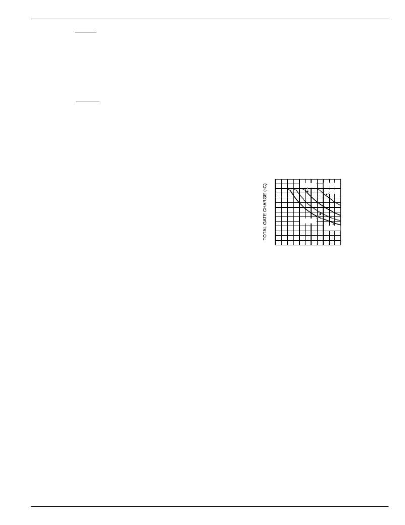
�The� graph� in� Figure� 7� shows� the� total� gate� charge� which� can�
�be� driven� by� the� MIC2185� over� the� input� voltage� range,� for�
�different� values� of� switching� frequency.�
�Frequency� vs.�
�Maximum� Gate� Charge�
�140�
�120�
�100�
�80�
�60�
�500kHz�
�40�
�20�
�0�
�INPUT� VOLTAGE� (V)�
�Figure� 7� -� MIC2185� Frequency� vs.� Max.� Gate� Charge�
�External� Schottky� Diode�
�An� external� boost� diode� in� parallel� with� the� high� side� MOSFET�
�is� used� to� keep� the� inductor� current� ?ow� continuous� during�
�the� non-overlap� time� when� both� MOSFETs� are� turned� off.�
�Although� the� average� current� through� this� diode� is� small,�
�the� diode� must� be� able� to� handle� currents� equal� to� the� peak�
�inductor� current.� This� peak� current� is� calculated� in� the� Cur-�
�rent� Limit� section� of� this� speci?cation�
�The� reverse� voltage� requirement� of� the� diode� is:�
�V� DIODE_RRM� =� V� OUT�
�For� the� MIC2185,� Schottky� diodes� with� a� 30V� or� 40V� rating�
�are� recommended.� Schottky� diodes� with� lower� reverse� volt-�
�age� ratings� have� higher� reverse� leakage� current� which� will�
�cause� ringing� and� excessive� power� dissipation� in� the� diode�
�and� low� side� MOSFET.�
�The� external� Schottky� diode� is� not� necessary� for� circuit�
�operation� since� the� high� side� MOSFET� contains� a� parasitic�
�body� diode.� However,� the� body� diode� has� a� relatively� slow�
�reverse� recovery� time� and� a� relatively� high� forward� voltage�
�drop.� The� lower� forward� voltage� drop� of� the� Schottky� diode�
�both� prevents� the� parasitic� diode� from� turning� on� and� im-�
�proves� ef?ciency.� The� lack� of� a� reverse� recovery� mechanism�
�in� a� Schottky� diode� causes� less� ringing� than� the� MOSFET's�
�parasitic� diode.� Depending� on� the� circuit� components� and�
�operating� conditions,� an� external� Schottky� diode� will� improve�
�the� converter� ef?ciency� by� 1� /� 2� %� to� 1%.�
�October� 2005�
�11�
�MIC2185�
�相关PDF资料 |
PDF描述 |
|---|---|
| MIC2184YM | IC REG CTRLR BUCK PWM CM 16-SOIC |
| SPD62-472M | INDUCTOR PWR SHIELDED 4.70UH SMD |
| LT3757IDD#PBF | IC REG CTRLR BST FLYBK INV 10DFN |
| MIC2182-5.0YM | IC REG CTRLR BUCK PWM CM 16-SOIC |
| LTC1622IS8#PBF | IC REG CTRLR BUCK PWM CM 8-SOIC |
相关代理商/技术参数 |
参数描述 |
|---|---|
| MIC2185YM TR | 功能描述:DC/DC 开关控制器 SO-16 Low Vin Synchronous Buck PWM Control IC (Lead Free) RoHS:否 制造商:Texas Instruments 输入电压:6 V to 100 V 开关频率: 输出电压:1.215 V to 80 V 输出电流:3.5 A 输出端数量:1 最大工作温度:+ 125 C 安装风格: 封装 / 箱体:CPAK |
| MIC2185YQS | 功能描述:DC/DC 开关控制器 SO-16 Low Vin Synchronous Buck PWM Control IC (Lead Free) RoHS:否 制造商:Texas Instruments 输入电压:6 V to 100 V 开关频率: 输出电压:1.215 V to 80 V 输出电流:3.5 A 输出端数量:1 最大工作温度:+ 125 C 安装风格: 封装 / 箱体:CPAK |
| MIC2185YQS TR | 功能描述:DC/DC 开关控制器 SO-16 Low Vin Synchronous Buck PWM Control IC (Lead Free) RoHS:否 制造商:Texas Instruments 输入电压:6 V to 100 V 开关频率: 输出电压:1.215 V to 80 V 输出电流:3.5 A 输出端数量:1 最大工作温度:+ 125 C 安装风格: 封装 / 箱体:CPAK |
| MIC2186 | 制造商:MICREL 制造商全称:Micrel Semiconductor 功能描述:Low Voltage PWM Control IC |
| MIC2186_05 | 制造商:MICREL 制造商全称:Micrel Semiconductor 功能描述:Low Voltage PWM Control IC |
发布紧急采购,3分钟左右您将得到回复。