- 您现在的位置:买卖IC网 > PDF目录15503 > MIC2185YM (Micrel Inc)IC REG CTRLR BST PWM CM 16-SOIC PDF资料下载
参数资料
| 型号: | MIC2185YM |
| 厂商: | Micrel Inc |
| 文件页数: | 12/15页 |
| 文件大小: | 0K |
| 描述: | IC REG CTRLR BST PWM CM 16-SOIC |
| 标准包装: | 48 |
| PWM 型: | 电流模式 |
| 输出数: | 1 |
| 频率 - 最大: | 440kHz |
| 占空比: | 95% |
| 电源电压: | 2.9 V ~ 14 V |
| 降压: | 无 |
| 升压: | 是 |
| 回扫: | 无 |
| 反相: | 无 |
| 倍增器: | 无 |
| 除法器: | 无 |
| Cuk: | 无 |
| 隔离: | 无 |
| 工作温度: | -40°C ~ 125°C |
| 封装/外壳: | 16-SOIC(0.154",3.90mm 宽) |
| 包装: | 管件 |
| 产品目录页面: | 1092 (CN2011-ZH PDF) |
| 其它名称: | 576-1714-5 MIC2185YM-ND |
�� �
�
�600ns�
�90� F� /2� LOW�
�80�
�6� F� /2� HIG� H�
�0�
�100� 200� 300� 400� 500� 600�
�MIC2185�
�Reference,� Enable� and� UVLO� Circuits�
�The� output� drivers� are� enabled� when� the� following� conditions�
�are� satis?ed:�
�?� The� VDD� voltage� (pin� 10)� is� greater� than� its�
�undervoltage� threshold.�
�?� The� voltage� on� the� Enable� pin� is� greater� than�
�the� Enable� /UVLO� threshold.�
�The� internal� bias� circuitry� generates� a� 1.245V� bandgap�
�reference� for� the� voltage� error� ampli?er� and� a� 3V� V� DD� volt-�
�age� for� the� internal� supply� bus.� The� reference� voltage� in� the�
�MIC2185� is� buffered� and� brought� out� to� pin� 8.� The� VREF�
�pin� must� be� bypassed� to� GND� (pin� 4)� with� a� 0.1μF� capaci-�
�tor.� The� VDD� pin� must� be� decoupled� to� ground� with� a� 1μF�
�ceramic� capacitor.�
�The� Enable� pin� (pin� 7)� has� two� threshold� levels,� allowing� the�
�MIC2185� to� shut� down� in� a� micro-current� mode,� or� turn� off�
�output� switching� in� standby� mode.� Below� 0.9V� (typical),� the�
�device� is� forced� into� a� low-power� shutdown.� If� the� enable� pin�
�is� between� 0.9V� and� 1.5V� (typical)� the� output� gate� drive� is�
�disabled� but� the� internal� circuitry� is� powered� on� and� the� soft�
�start� pin� voltage� is� forced� low.� There� is� typically� 140mV� of�
�hysteresis� below� the� 1.5V� threshold� to� insure� the� part� does�
�not� oscillate� on� and� off� due� to� ripple� voltage� on� the� input.�
�Raising� the� Enable� voltage� above� the� UVLO� threshold� of� 1.5V�
�enables� the� output� drivers� and� allows� the� soft� start� capacitor�
�to� charge.� The� Enable� pin� may� be� pulled� up� to� V� IN� A.�
�Oscillator� &� Sync�
�The� internal� oscillator� is� self-contained� and� requires� no�
�external� components.� The� f/2� pin� allows� the� user� to� select�
�from� two� switching� frequencies.� A� low� level� sets� the� oscilla-�
�tor� frequency� to� 400kHz� and� a� high� level� sets� the� oscillator�
�frequency� to� 200kHz.� The� maximum� duty� cycle� for� both�
�frequencies� is� typically� 85%.� The� minimum� pulse� width� in-�
�creases� but� does� not� double� when� the� frequency� is� changed�
�from� 400kHz� to� 200kHz.� This� means� the� minimum� duty� cycle�
�is� slightly� lower� at� 200kHz.� This� may� be� important� as� the�
�input� voltage� approaches� the� output� voltage.� At� lower� duty�
�cycles,� the� input� voltage� can� be� closer� to� the� output� voltage�
�without� the� output� rising� out� of� regulation.�
�A� frequency� foldback� mode� is� enabled� if� the� voltage� on� the�
�Feedback� pin� (pin� 6)� is� less� than� 0.3V.� In� frequency� foldback�
�the� oscillator� frequency� is� reduced� by� approximately� a� factor�
�of� 4.� For� the� 400kHz� setting,� the� oscillator� runs� at� 100khz� in�
�frequency� foldback.� For� a� 200kHz� setting� the� oscillator� runs�
�at� approximately� 50kHz.�
�The� SYNC� input� (pin� 11)� allows� the� MIC2185� to� synchronize�
�with� an� external� CMOS� or� TTL� clock� signal.� The� rising� edge�
�of� the� sync� signal� generates� a� reset� signal� in� the� oscillator,�
�which� turns� off� the� high� side� gate� drive� output.� The� low� side-�
�drive� then� turns� on,� restarting� the� switching� cycle.� The� sync�
�signal� is� inhibited� when� the� controller� operates� in� skip� mode�
�or� frequency� foldback.� The� sync� signal� frequency� must� be�
�greater� than� the� maximum� speci?ed� free� running� frequency� of�
�the� MIC2185.� If� the� synchronizing� frequency� is� lower,� double�
�pulsing� of� the� gate� drive� outputs� will� occur.� When� not� used,�
�the� sync� pin� must� be� connected� to� ground.�
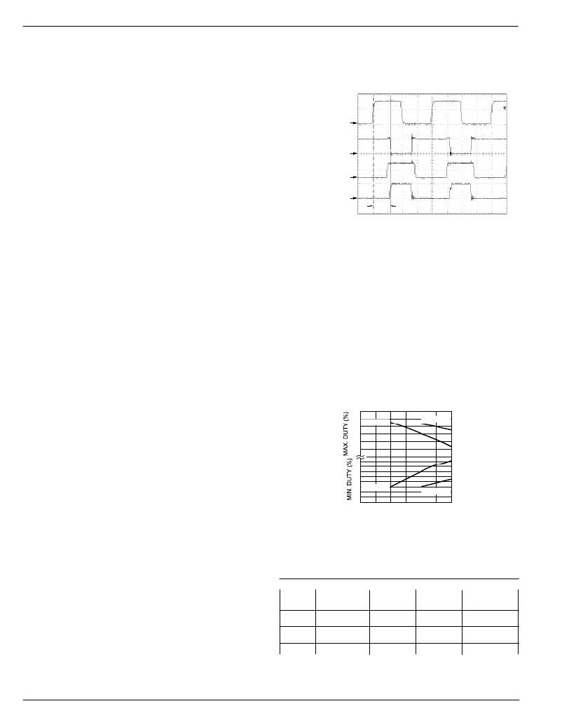
�Figure� 8� shows� the� timing� between� the� external� sync� signal,�
�Micrel,� Inc.�
�low� side-drive� and� the� high� side� drive� when� the� f/2� pin� is� low.�
�The� delay� between� the� rising� edge� of� the� sync� signal� and� the�
�turn� on� of� the� low� side� gate� drive� is� typically� 900ns� when� the�
�f/2� pin� is� high� and� 600ns� when� the� f/2� pin� is� low.�
�Sync� Waveform�
�Sync� Input�
�2V/div�
�Switch� NodeVoltage�
�(Low� Side� FET� Drain)�
�5V/div�
�High� Side� FET�
�Gate� Drive�
�5V/div�
�Low� Side� FET�
�Gate� Drive�
�5V/div�
�TIME� (500ns/div)�
�Figure� 8.� Sync� Waveforms�
�The� maximum� recommended� output� switching� frequency� is�
�600kHz.� Synchronizing� to� higher� frequencies� may� be� pos-�
�sible,� however� there� are� some� concerns.� As� the� switching�
�frequency� is� increased,� the� switching� period� decreases.�
�The� minimum� on� time� in� the� MIC2185� becomes� a� greater�
�part� of� the� total� switching� period.� This� may� prevent� proper�
�operation� as� Vin� approaches� Vout� and� may� also� minimize�
�the� effectiveness� of� the� current� limit� circuitry.� The� maximum�
�duty� cycle� decreases� as� the� sync� frequency� is� increased.�
�Figure� 9� shows� the� relationship� between� the� minimum� and�
�maximum� duty� cycle� and� frequency.�
�MIC2185� Sync� Frequency�
�vs.� Duty� cycle�
�100�
�F� /2� HIG� H�
�18�
�70�
�60�
�50�
�40�
�16�
�14�
�12�
�10�
�8�
�4� F� /2� LOW�
�2�
�0�
�FREQUENCY� (kHz)�
�Figure� 9�
�Table� 1� summarizes� the� differences� in� the� MIC2185� for� the�
�two� different� states� of� the� f/2� pin.�
�F/2� pin� Switching� Typical� Typical� t� OFF� in�
�Level� Frequency� Max� Duty� Min.� Duty� SKIP� Mode�
�(kHz)� cycle� (%)� cycle� (%)�
�0� 400� 85� 6� 1μs�
�1� 200� 85� 6� 2μs�
�MIC2185� Table� 1�
�MIC2185�
�12�
�October� 2005�
�相关PDF资料 |
PDF描述 |
|---|---|
| MIC2184YM | IC REG CTRLR BUCK PWM CM 16-SOIC |
| SPD62-472M | INDUCTOR PWR SHIELDED 4.70UH SMD |
| LT3757IDD#PBF | IC REG CTRLR BST FLYBK INV 10DFN |
| MIC2182-5.0YM | IC REG CTRLR BUCK PWM CM 16-SOIC |
| LTC1622IS8#PBF | IC REG CTRLR BUCK PWM CM 8-SOIC |
相关代理商/技术参数 |
参数描述 |
|---|---|
| MIC2185YM TR | 功能描述:DC/DC 开关控制器 SO-16 Low Vin Synchronous Buck PWM Control IC (Lead Free) RoHS:否 制造商:Texas Instruments 输入电压:6 V to 100 V 开关频率: 输出电压:1.215 V to 80 V 输出电流:3.5 A 输出端数量:1 最大工作温度:+ 125 C 安装风格: 封装 / 箱体:CPAK |
| MIC2185YQS | 功能描述:DC/DC 开关控制器 SO-16 Low Vin Synchronous Buck PWM Control IC (Lead Free) RoHS:否 制造商:Texas Instruments 输入电压:6 V to 100 V 开关频率: 输出电压:1.215 V to 80 V 输出电流:3.5 A 输出端数量:1 最大工作温度:+ 125 C 安装风格: 封装 / 箱体:CPAK |
| MIC2185YQS TR | 功能描述:DC/DC 开关控制器 SO-16 Low Vin Synchronous Buck PWM Control IC (Lead Free) RoHS:否 制造商:Texas Instruments 输入电压:6 V to 100 V 开关频率: 输出电压:1.215 V to 80 V 输出电流:3.5 A 输出端数量:1 最大工作温度:+ 125 C 安装风格: 封装 / 箱体:CPAK |
| MIC2186 | 制造商:MICREL 制造商全称:Micrel Semiconductor 功能描述:Low Voltage PWM Control IC |
| MIC2186_05 | 制造商:MICREL 制造商全称:Micrel Semiconductor 功能描述:Low Voltage PWM Control IC |
发布紧急采购,3分钟左右您将得到回复。