- 您现在的位置:买卖IC网 > PDF目录15332 > MIC2186YM TR (Micrel Inc)IC REG CTRLR BST FLYBK CM 16SOIC PDF资料下载
参数资料
| 型号: | MIC2186YM TR |
| 厂商: | Micrel Inc |
| 文件页数: | 11/15页 |
| 文件大小: | 0K |
| 描述: | IC REG CTRLR BST FLYBK CM 16SOIC |
| 标准包装: | 2,500 |
| PWM 型: | 电流模式 |
| 输出数: | 1 |
| 频率 - 最大: | 440kHz |
| 占空比: | 85% |
| 电源电压: | 2.9 V ~ 14 V |
| 降压: | 无 |
| 升压: | 是 |
| 回扫: | 是 |
| 反相: | 无 |
| 倍增器: | 无 |
| 除法器: | 无 |
| Cuk: | 无 |
| 隔离: | 无 |
| 工作温度: | -40°C ~ 125°C |
| 封装/外壳: | 16-SOIC(0.154",3.90mm 宽) |
| 包装: | 带卷 (TR) |
| 其它名称: | MIC2186YMTR MIC2186YMTR-ND |
�� �
�
�MIC2186�
�Micrel,� Inc.�
�R� SENSE� =�
�V� SENSE�
�I� IND(pk)�
�switching� cycle.� A� small� RC� filter� between� the� current� sense�
�pin� and� current� sense� resistor� may� help� to� attenuate� larger�
�switching� spikes� or� high� frequency� switching� noise.� Adding�
�where:�
�Vsense� is� the� minimum� current� sense� threshold�
�of� the� CSH� pin�
�Maximum� Peak� Current� in� Continuous� Mode:�
�The� peak� inductor� current� is� equal� to� the� average� inductor�
�current� plus� one� half� of� the� peak� to� peak� inductor� current.�
�The� peak� inductor� current� is:�
�the� filter� slows� down� the� current� sense� signal,� which� has� the�
�effect� of� slightly� raising� the� overcurrent� limit� threshold.�
�MOSFET� Gate� Drive�
�The� MIC2186� converter� drives� a� low� side� N-channel� MOSFET.�
�The� driver� for� the� OutN� pin� has� a� 1.6� ?� typical� source� and� sink�
�impedance.� The� VinP� pin� is� the� supply� pin� for� the� gate� drive�
�circuit.� It� typically� connected� to� the� output.� The� maximum�
�supply� voltage� to� the� VinP� pin� is� 14V.� If� the� output� voltage� is�
�I� IND(pk)� =� O� O� +�
�� I� IND(pp)�
�I� IND(pk)� =� I� IND(ave)� +�
�V� � I�
�V� IN� ×� η�
�1�
�2�
�V� L� ×� (� V� O� ?� V� IN� ×� η� )�
�2� � V� O� � fs� � L�
�greater� than� 14V� or� if� it� is� desired� to� drive� the� MOSFET� with�
�a� voltage� less� than� Vout,� the� VinP� pin� can� be� connected� to� the�
�input� or� to� an� separate� supply� voltage.�
�MOSFET� Selection�
�In� a� boost� converter,� the� Vds� of� the� MOSFET� is� approxi-�
�where:�
�Io� is� the� maximum� output� current�
�Vo� is� the� output� voltage�
�Vin� is� the� minimum� input� voltage�
�L� is� the� value� of� the� boost� inductor�
�fs� is� the� switching� frequency�
�η� is� the� efficiency� of� the� boost� converter�
�VL� is� the� voltage� across� the� inductor�
�VL� may� be� approximated� as� Vin� for� higher� input� voltage.�
�However,� the� voltage� drop� across� the� inductor� winding� resis-�
�tance� and� low� side� MOSFET� on-resistance� must� be� ac-�
�counted� for� at� the� lower� input� voltages� that� the� MIC2186�
�operates� at.�
�mately� equal� to� the� output� voltage.� The� maximum� Vds� rating�
�of� the� MOSFET� must� be� high� enough� to� allow� for� ringing� and�
�spikes� in� addition� to� the� output� voltage.�
�The� VinP� pin� supplies� the� N-channel� gate� drive� voltage.� The�
�Vgs� threshold� voltage� of� the� N-channel� MOSFET� must� be� low�
�enough� to� operate� at� the� minimum� VinP� voltage� to� guarantee�
�the� boost� converter� will� start� up.�
�The� maximum� amout� of� MOSFET� gate� charge� that� can� be�
�driven� is� limited� by� the� power� dissipation� in� the� MIC2186.� The�
�power� dissipated� by� the� gate� drive� circuitry� is� calculated�
�below:�
�P_gate_drive=Q_gate� *� VinP� *� fs�
�where:�
�Q_gate� is� the� total� gate� charge� of� the� external�
�(�
�V� L� IN� ?� O� O� � R� WINDING� DSON�
�=� V� +� R�
�V� � I�
�V� IN� ×� η�
�)�
�MOSFET�
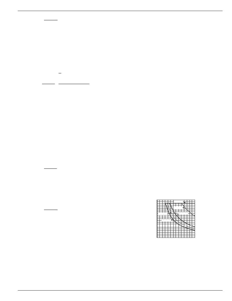
�The� graph� in� Figure� 7� shows� the� total� gate� charge� which� can�
�be� driven� by� the� MIC2186� over� the� input� voltage� range,� for�
�where:�
�Rwinding� is� the� winding� resistance� of� the� inductor�
�Rdson� is� the� on� resistance� of� the� low� side� switching�
�different� values� of� switching� frequency.� Higher� gate� charge�
�will� slow� down� the� turn-on� and� turn-off� times� of� the� MOSFET,�
�which� increases� switching� losses.�
�MOSFET�
�The� maximum� value� of� current� sense� resistor� is:�
�220�
�200�
�Power� Dissipation�
�vs.� Frequency�
�100kHz�
�R� SENSE� =�
�V� SENSE�
�I� IND(pk)�
�180�
�160�
�140� 500kHz�
�200kHz�
�400kHz�
�120�
�where:�
�V� SENSE� is� the� minimum� current� sense� threshold�
�of� the� CSH� pin�
�100�
�80�
�60�
�40�
�600kHz�
�0� 2� 4� 6� 8� 10�
�Thecurrentsensepin,CSH,isnoisesensitiveduetothelow�
�signal� level.� The� current� sense� voltage� measurement� is�
�20�
�0�
�V� IN� P� (V)�
�12�
�14�
�referenced� to� the� signal� ground� pin� of� the� MIC2186.� The�
�current� sense� resistor� ground� should� be� located� close� to� the�
�IC� ground.� Make� sure� there� are� no� high� currents� flowing� in� this�
�trace.� The� PCB� trace� between� the� high� side� of� the� current�
�sense� resistor� and� the� CHS� pin� should� also� be� short� and�
�routed� close� to� the� ground� connection.� The� input� to� the�
�internal� current� sense� amplifier� has� a� 30nS� dead� time� at� the�
�beginning� of� each� switching� cycle.� This� dead� time� prevents�
�leading� edge� current� spikes� from� prematurely� terminating� the�
�Figure� 7� -� MIC2186� freq� vs� pdiss�
�External� Schottky� Diode�
�In� a� boost� converter� topology,� the� boost� diode,� D1� must� be�
�rated� to� handle� the� peak� and� average� current.� The� average�
�current� through� the� diode� is� equal� to� the� average� output�
�current� of� the� boost� converter.� The� peak� current� is� calculated�
�in� the� current� limit� section� of� this� specification.�
�April� 2005�
�11�
�M9999-042205�
�相关PDF资料 |
PDF描述 |
|---|---|
| ASM10DRYH-S13 | CONN EDGECARD 20POS .156 EXTEND |
| UPM1E152MHD | CAP ALUM 1500UF 25V 20% RADIAL |
| MIC2185YM TR | IC REG CTRLR BST PWM CM 16-SOIC |
| IDCS2512ER152M | INDUCTOR POWER 1500UH 0.12A SMD |
| MIC2184YM TR | IC REG CTRLR BUCK PWM CM 16-SOIC |
相关代理商/技术参数 |
参数描述 |
|---|---|
| MIC2186YQS | 功能描述:DC/DC 开关控制器 SO-16 Low Vin Synchronous Buck PWM Control IC (Lead Free) RoHS:否 制造商:Texas Instruments 输入电压:6 V to 100 V 开关频率: 输出电压:1.215 V to 80 V 输出电流:3.5 A 输出端数量:1 最大工作温度:+ 125 C 安装风格: 封装 / 箱体:CPAK |
| MIC2186YQS TR | 功能描述:DC/DC 开关控制器 SO-16 Low Vin Synchronous Buck PWM Control IC (Lead Free) RoHS:否 制造商:Texas Instruments 输入电压:6 V to 100 V 开关频率: 输出电压:1.215 V to 80 V 输出电流:3.5 A 输出端数量:1 最大工作温度:+ 125 C 安装风格: 封装 / 箱体:CPAK |
| MIC2193 | 制造商:MICREL 制造商全称:Micrel Semiconductor 功能描述:400KHZ SO 8 SYNCHRONOUS BUCK CONTROL IC |
| MIC2193BM | 功能描述:IC REG CTRLR BUCK PWM CM 8-SOIC RoHS:否 类别:集成电路 (IC) >> PMIC - 稳压器 - DC DC 切换控制器 系列:- 标准包装:4,000 系列:- PWM 型:电压模式 输出数:1 频率 - 最大:1.5MHz 占空比:66.7% 电源电压:4.75 V ~ 5.25 V 降压:是 升压:无 回扫:无 反相:无 倍增器:无 除法器:无 Cuk:无 隔离:无 工作温度:-40°C ~ 85°C 封装/外壳:40-VFQFN 裸露焊盘 包装:带卷 (TR) |
| MIC2193BM TR | 功能描述:IC REG CTRLR BUCK PWM CM 8-SOIC RoHS:否 类别:集成电路 (IC) >> PMIC - 稳压器 - DC DC 切换控制器 系列:- 标准包装:4,000 系列:- PWM 型:电压模式 输出数:1 频率 - 最大:1.5MHz 占空比:66.7% 电源电压:4.75 V ~ 5.25 V 降压:是 升压:无 回扫:无 反相:无 倍增器:无 除法器:无 Cuk:无 隔离:无 工作温度:-40°C ~ 85°C 封装/外壳:40-VFQFN 裸露焊盘 包装:带卷 (TR) |
发布紧急采购,3分钟左右您将得到回复。