- 您现在的位置:买卖IC网 > PDF目录14545 > MIC2295YD5 TR (Micrel Inc)IC REG BOOST ADJ 1.2A TSOT23-5 PDF资料下载
参数资料
| 型号: | MIC2295YD5 TR |
| 厂商: | Micrel Inc |
| 文件页数: | 9/12页 |
| 文件大小: | 0K |
| 描述: | IC REG BOOST ADJ 1.2A TSOT23-5 |
| 标准包装: | 1 |
| 类型: | 升压(升压) |
| 输出类型: | 可调式 |
| 输出数: | 1 |
| 输出电压: | 最高 34V |
| 输入电压: | 2.5 V ~ 10 V |
| PWM 型: | 电流模式 |
| 频率 - 开关: | 1.2MHz |
| 电流 - 输出: | 1.2A |
| 同步整流器: | 无 |
| 工作温度: | -40°C ~ 125°C |
| 安装类型: | 表面贴装 |
| 封装/外壳: | SOT-23-5 细型,TSOT-23-5 |
| 包装: | 标准包装 |
| 供应商设备封装: | TSOT-23-5 |
| 产品目录页面: | 1093 (CN2011-ZH PDF) |
| 其它名称: | 576-1080-6 |
�� �
�
�10mH�
�V� OUT�
�V� IN�
�Micrel�
�Application� Information�
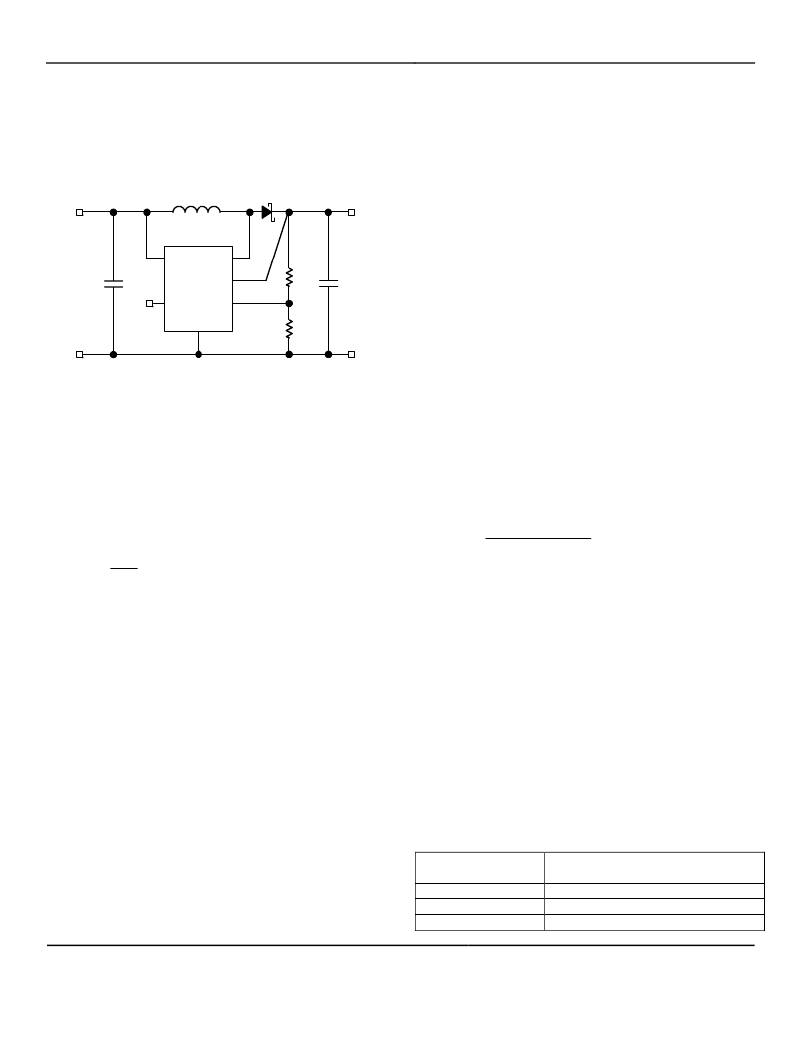
�DC� to� DC� PWM� Boost� Conversion�
�The� MIC2295� is� a� constant� frequency� boost� converter.� It�
�operates� by� taking� a� DC� input� voltage� and� regulating� a�
�higher� DC� output� voltage.� Figure� 2� shows� a� typical� circuit.�
�L1�
�D1�
�MIC2288BML�
�MIC2295�
�components.� To� ensure� the� highest� level� of� protection,� the�
�MIC2295� OVP� pin� will� shut� the� switch� off� when� an� over-�
�voltage� condition� is� detected� saving� itself� and� other�
�sensitive� circuitry� downstream.�
�Component� Selection�
�Inductor�
�Inductor� selection� is� a� balance� between� efficiency,�
�stability,� cost,� size� and� rated� current.� For� most� applications�
�a� 10μH� is� the� recommended� inductor� value.� It� is� usually� a�
�good� balance� between� these� considerations.� Efficiency� is�
�C1�
�2.2μF�
�VIN�
�EN�
�SW�
�OVP�
�FB�
�R1�
�C2�
�10μF�
�affected� by� inductance� value� in� that� larger� inductance�
�values� reduce� the� peak� to� peak� ripple� current.� This� has� an�
�effect� of� reducing� both� the� DC� losses� and� the� transition�
�losses.�
�GND�
�GND�
�R2�
�GND�
�There� is� also� a� secondary� effect� of� an� inductors� DC�
�resistance� (DCR).� The� DCR� of� an� inductor� will� be� higher�
�for� more� inductance� in� the� same� package� size.� This� is� due�
�V� IN�
�V� IN� 2�
�V� OUT� ×� L� ×� I� OUT� ×� 2� π�
�Figure� 2�
�Boost� regulation� is� achieved� by� turning� on� an� internal�
�switch,� which� draws� current� through� the� inductor� (L1).�
�When� the� switch� turns� off,� the� inductor’s� magnetic� field�
�collapses,� causing� the� current� to� be� discharged� into� the�
�output� capacitor� through� an� external� Schottkey� diode� (D1).�
�Voltage� regulation� is� achieved� my� modulating� the� pulse�
�width� or� pulse� width� modulation� (PWM).�
�Duty� Cycle� Considerations�
�Duty� cycle� refers� to� the� switch� on-to-off� time� ratio� and� can�
�be� calculated� as� follows� for� a� boost� regulator;�
�D� =� 1� ?�
�V� OUT�
�The� duty� cycle� required� for� voltage� conversion� should� be�
�less� than� the� maximum� duty� cycle� of� 85%.� Also,� in� light�
�load� conditions� where� the� input� voltage� is� close� to� the�
�output� voltage,� the� minimum� duty� cycle� can� cause� pulse�
�skipping.� This� is� due� to� the� energy� stored� in� the� inductor�
�causing� the� output� to� overshoot� slightly� over� the� regulated�
�output� voltage.� During� the� next� cycle,� the� error� amplifier�
�detects� the� output� as� being� high� and� skips� the� following�
�pulse.� This� effect� can� be� reduced� by� increasing� the�
�minimum� load� or� by� increasing� the� inductor� value.�
�Increasing� the� inductor� value� reduces� peak� current,� which�
�in� turn� reduces� energy� transfer� in� each� cycle.�
�Over� Voltage� Protection�
�For� MLF� package� of� MIC2295,� there� is� an� over� voltage�
�to� the� longer� windings� required� for� an� increase� in�
�inductance.� Since� the� majority� of� input� current� (minus� the�
�MIC2295� operating� current)� is� passed� through� the�
�inductor,� higher� DCR� inductors� will� reduce� efficiency.�
�Also,� to� maintain� stability,� increasing� inductor� size� will�
�have� to� be� met� with� an� increase� in� output� capacitance.�
�This� is� due� to� the� unavoidable� “right� half� plane� zero”� effect�
�for� the� continuous� current� boost� converter� topology.� The�
�frequency� at� which� the� right� half� plane� zero� occurs� can� be�
�calculated� as� follows;�
�Frhpz� =�
�The� right� half� plane� zero� has� the� undesirable� effect� of�
�increasing� gain,� while� decreasing� phase.� This� requires� that�
�the� loop� gain� is� rolled� off� before� this� has� significant� effect�
�on� the� total� loop� response.� This� can� be� accomplished� by�
�either� reducing� inductance� (increasing� RHPZ� frequency)� or�
�increasing� the� output� capacitor� value� (decreasing� loop�
�gain).�
�Output� Capacitor�
�Output� capacitor� selection� is� also� a� trade-off� between�
�performance,� size� and� cost.� Increasing� output� capacitance�
�will� lead� to� an� improved� transient� response,� but� also� an�
�increase� in� size� and� cost.� X5R� or� X7R� dielectric� ceramic�
�capacitors� are� recommended� for� designs� with� the�
�MIC2295.� Y5V� values� may� be� used,� but� to� offset� their�
�tolerance� over� temperature,� more� capacitance� is� required.�
�The� following� table� shows� the� recommended� ceramic�
�protection� function.� If� the�
�feedback� resistors� are�
�(X5R)� output� capacitor� value� vs.� output� voltage.�
�disconnected� from� the� circuit� or� the� feedback� pin� is�
�shorted� to� ground,� the� feedback� pin� will� fall� to� ground�
�potential.� This� will� cause� the� MIC2295� to� switch� at� full�
�duty-cycle� in� an� attempt� to� maintain� the� feedback� voltage.�
�As� a� result� the� output� voltage� will� climb� out� of� control.� This�
�may� cause� the� switch� node� voltage� to� exceed� its� maximum�
�voltage� rating,� possibly� damaging� the� IC� and� the� external�
�April� 2005�
�9�
�Output� Voltage�
�<6V�
�<16V�
�<34V�
�Recommended� Output�
�Capacitance�
�10μF�
�4.7μF�
�2.2μF�
�M9999-042605�
�(408)� 955-1690�
�相关PDF资料 |
PDF描述 |
|---|---|
| ASC08DRTN | CONN EDGECARD 16POS .100 DIP SLD |
| ASC08DRTH | CONN EDGECARD 16POS .100 DIP SLD |
| RCM06DTBD-S664 | CONN EDGECARD 12POS R/A .156 |
| RCM06DTMN-S664 | CONN EDGECARD 12POS R/A .156 |
| MIC2296YML TR | IC REG BOOST ADJ 1.2A 8MLF |
相关代理商/技术参数 |
参数描述 |
|---|---|
| MIC2295YML | 制造商:MICREL 制造商全称:Micrel Semiconductor 功能描述:High Power Density 1.2A Boost Regulator |
| MIC2295YML TR | 功能描述:直流/直流开关转换器 1.2MHz 1.2A PWM Boost Converter (Lead Free) RoHS:否 制造商:STMicroelectronics 最大输入电压:4.5 V 开关频率:1.5 MHz 输出电压:4.6 V 输出电流:250 mA 输出端数量:2 最大工作温度:+ 85 C 安装风格:SMD/SMT |
| MIC2295YML-TR | 功能描述:Boost Switching Regulator IC Positive Adjustable 2.5V 1 Output 1.2A (Switch) 8-VFDFN Exposed Pad, 8-MLF? 制造商:microchip technology 系列:- 包装:剪切带(CT) 零件状态:有效 功能:升压 输出配置:正 拓扑:升压 输出类型:可调式 输出数:1 电压 - 输入(最小值):2.5V 电压 - 输入(最大值):10V 电压 - 输出(最小值/固定):2.5V 电压 - 输出(最大值):34V(开关) 电流 - 输出:1.2A(开关) 频率 - 开关:1.2MHz 同步整流器:无 工作温度:-40°C ~ 125°C (TJ) 安装类型:表面贴装 封装/外壳:8-VFDFN 裸露焊盘,8-MLF? 供应商器件封装:8-MLF?(2x2) 标准包装:1 |
| MIC2296 | 制造商:MICREL 制造商全称:Micrel Semiconductor 功能描述:High Power Density 1.2A Boost Regulator |
| MIC2296_10 | 制造商:MICREL 制造商全称:Micrel Semiconductor 功能描述:High Power Density 1.2A Boost Regulator |
发布紧急采购,3分钟左右您将得到回复。