参数资料
| 型号: | MIC2550ABML TR |
| 厂商: | Micrel Inc |
| 文件页数: | 10/11页 |
| 文件大小: | 0K |
| 描述: | IC USB TRANSCEIVER 16-MLF |
| 标准包装: | 5,000 |
| 类型: | USB 收发器 |
| 驱动器/接收器数: | 1/1 |
| 规程: | USB 2.0 |
| 电源电压: | 4 V ~ 5.25 V |
| 安装类型: | 表面贴装 |
| 封装/外壳: | 16-VQFN Exposed Pad,16-MLF? |
| 供应商设备封装: | 16-MLF?(4x4) |
| 包装: | 带卷 (TR) |
| 其它名称: | MIC2550ABMLTR MIC2550ABMLTR-ND |
MIC2550A
Micrel, Inc.
M9999-031805
8
March 2005
Applications Information
The MIC2550A is designed to provide USB connectivity in
mobile systems where system supply voltages are not avail-
able to satisfy USB requirements. The MIC2550A can oper-
ate down to supply voltages of 2.5V and still meet USB
physical layer specifications. As shown in the system dia-
gram, the MIC2550A takes advantage of USB’s supply
voltage, V
BUS, to operate the transceiver. The system volt-
age, V
IF, is used to set the reference voltage used by the
digital I/O lines (VP, VM, RCV, OE#, SPD, and SUS pins)
interfacing to the system. Internal circuitry provides transla-
tion between the USB and system voltage domains. V
IF will
typically be the main supply voltage rail for the system.
In addition, a 3.3V, 10% termination supply voltage, V
TRM, is
provided to support speed selection. A 0.47F (minimum)
capacitor from V
TRM to ground is required to ensure stability.
A 1.5K resistor is required between this pin and the D+ or D–
lines to respectively specify full-speed or low-speed opera-
tion.
Power Supply Configurations
V
IF /VBUS Switched
When the V
BUS input pin is pulled to ground a low impedance
path between V
IF and VBUS can cause a high current flow
from V
IF to VBUS thereby damaging the MIC2550A. This
issue can arise in systems where V
BUS is driven from a power
supply that can be switched off such as in the case of a
desktop PC. Adding a Schottky diode, such as the ZHCS1000
by Zetex, in series with V
BUS will prevent any current flow
during this condition. A solution is shown in Figure 8 below.
If the V
IF source is current limited to less than 50mA, then
diode D1 is not necessary.
MIC2550
VIF
Note: *(Optional) See Text - Power Supply Configurations
VBUS
1F min
VBUS
USB Device
Power Controller
*(Optional)
D1
ZHCS1000 or
equivalent
Figure 8. Solution to V
IF /VBUS Switching
I/O Interface Using 3.3V
In systems where the I/O interface utilizes a 3.3V USB
controller, an alternate solution is shown in Figure 9. This
configuration has the advantage over Figure 8, in that no
extra components are needed. Ensure that the load on V
TRM
does not exceed 1mA total.
MIC2550
VIF
VBUS
I/O
VBUS
VP/VM/
RCV/OE#
VTRM
USB
Controller
VDD
3.3V
Figure 9. I/O Interface Using 3.3V
Internal 3.3V Source
If the device is self-powered and has 3.3V available, the
circuit in Figure 10 is yet another power supply configuration
option. In this configuration, the internal regulator is disabled
and the 3.3V source and not V
BUS powers the entire chip.
MIC2550A
VIF
3.3V
VBUS
VTRM
Figure 10. Powering Chip
from Internal 3.3V Source
Suspend
When the suspend pin (SUS) is high, power consumption is
reduced to a minimum. V
TRM is not disabled. RCV, VP and VM
are still functional to enable the device to detect USB activity.
For minimal current consumption in suspend mode, it is
recommended that OE# = 1, and SPD = 0.
Speed
The speed pin (SPD) sets D+/D– output edge rates by increas-
ing or decreasing biasing current sources within the output
drivers. For low speed, SPD = 0. For full speed, SPD = 1. By
setting SPD = 0 during idle periods, in conjunction with suspend
(SUS), the lowest quiescent current can be obtained. However,
designers must provide a 300ns delay between changing SPD
from 0 to 1 and transmission of data at full speed. This delay
ensures the output drivers have arrived at their proper operating
conditions. Failure to do so can result in leading edge distortion
on the first few data bits transmitted.
External ESD Protection
The use of ESD transient protection devices is not required
for operation, but is recommended. We recommend the
following devices or the equivalent:
Cooper Electronics Technologies (www.cooperet.com)
41206ESDA SurgX
0805ESDA SurgX
Littelfuse (www.littlefuse.com)
V0402MHS05
SP0503BAHT
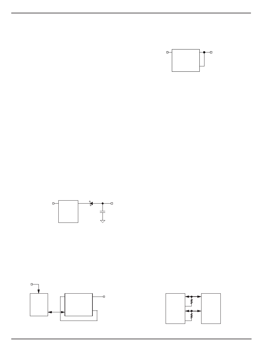
Non-multiplexed Bus
To save pin count for the USB logic controller interface, the
MIC2550A was designed with V
P and VM as bidirectional
pins. To interface the MIC2550A with a non-multiplexed data
bus, resistors can be used for low cost isolation as shown in
Figure 11.
VPO
VP
VM
VMO
USB Logic
Controller
(SIE)
MIC2550
VP
VM
10k
Figure 11. MIC2550A Interface to
Non-multiplexed Data Bus
相关PDF资料 |
PDF描述 |
|---|---|
| VE-27T-MX-F4 | CONVERTER MOD DC/DC 6.5V 75W |
| MS27466T21B41S | CONN RCPT 41POS WALL MT W/SCKT |
| VE-27R-MX-F4 | CONVERTER MOD DC/DC 7.5V 75W |
| VI-JT2-MX-F4 | CONVERTER MOD DC/DC 15V 75W |
| VI-JT2-MX-F3 | CONVERTER MOD DC/DC 15V 75W |
相关代理商/技术参数 |
参数描述 |
|---|---|
| MIC2550ABTS | 功能描述:IC USB TRANSCEIVER 14-TSSOP RoHS:否 类别:集成电路 (IC) >> 接口 - 驱动器,接收器,收发器 系列:- 标准包装:1,140 系列:AU 类型:收发器 驱动器/接收器数:1/1 规程:CAN 电源电压:5.3 V ~ 27 V 安装类型:表面贴装 封装/外壳:14-SOIC(0.154",3.90mm 宽) 供应商设备封装:14-SO 包装:管件 其它名称:935267940512AU5790D14AU5790D14-ND |
| MIC2550ABTS TR | 功能描述:IC USB TRANSCEIVER 14-TSSOP RoHS:否 类别:集成电路 (IC) >> 接口 - 驱动器,接收器,收发器 系列:- 标准包装:1,140 系列:AU 类型:收发器 驱动器/接收器数:1/1 规程:CAN 电源电压:5.3 V ~ 27 V 安装类型:表面贴装 封装/外壳:14-SOIC(0.154",3.90mm 宽) 供应商设备封装:14-SO 包装:管件 其它名称:935267940512AU5790D14AU5790D14-ND |
| MIC2550AYML | 制造商:Rochester Electronics LLC 功能描述: 制造商:RF Micro Devices Inc 功能描述: |
| MIC2550AYML TR | 功能描述:USB 接口集成电路 USB Transceiver - Lead Free RoHS:否 制造商:Cypress Semiconductor 产品:USB 2.0 数据速率: 接口类型:SPI 工作电源电压:3.15 V to 3.45 V 工作电源电流: 最大工作温度:+ 85 C 安装风格:SMD/SMT 封装 / 箱体:WLCSP-20 |
| MIC2550AYML25 TR | 功能描述:USB 接口集成电路 USB Transceiver - Lead Free RoHS:否 制造商:Cypress Semiconductor 产品:USB 2.0 数据速率: 接口类型:SPI 工作电源电压:3.15 V to 3.45 V 工作电源电流: 最大工作温度:+ 85 C 安装风格:SMD/SMT 封装 / 箱体:WLCSP-20 |
发布紧急采购,3分钟左右您将得到回复。