参数资料
| 型号: | MIC2551ABTS TR |
| 厂商: | Micrel Inc |
| 文件页数: | 10/11页 |
| 文件大小: | 0K |
| 描述: | IC USB TRANSCEIVER 14-TSSOP |
| 标准包装: | 2,500 |
| 类型: | USB 收发器 |
| 驱动器/接收器数: | 1/1 |
| 规程: | USB 2.0 |
| 电源电压: | 4 V ~ 5.25 V |
| 安装类型: | 表面贴装 |
| 封装/外壳: | 14-TSSOP(0.173",4.40mm 宽) |
| 供应商设备封装: | 14-TSSOP |
| 包装: | 带卷 (TR) |
| 其它名称: | MIC2551ABTSTR MIC2551ABTSTR-ND |
MIC2551
Micrel, Inc.
M9999-112008
8
November 2008
Application Information
Power Supply Configuration
The MIC2551 can be set up for different power supply
configurations which modify the behavior of the device. Both
V
BUS and VIF have special thresholds that detect when they
are either removed or grounded. Table 3 depicts the behavior
under the different power supply configuration scenarios that
are explained below.
Normal Mode
V
BUS is connected to the 5.0V USB bus voltage and VIF is
connected to a supply voltage in the range of 1.6V to 3.6V. In
this case V
TRM supplies a 3.3V voltage for powering the
speed select resistor via V
PU depending on the state of the
CON pin.
Disconnect Mode
V
IF is connected to a supply in a range of 1.6V to 3.6V and
V
BUS is open or grounded. If VBUS is opened while transmit-
ting, the data lines (D+, D–) have sharing capability and may
be driven with external devices up to approximately 3.6V if,
and only if, SUSPEND is enabled (SUS = 1). With V
BUS
ground, D+, D– sharing mode is not permitted.
Disable Mode
V
BUS is connected to the 5.0V USB bus voltage and VIF is
open. All logic controlled inputs become high impedances,
thus minimal current will be supplied by V
IF if the input pins are
pulled up to an external source.
Alternate Power Supply Configuration Options
I/O Interface Using 3.3V
In systems where the I/O interface utilizes a 3.3V USB
controller, an alternate solution is shown in Figure 7. No extra
components are required; however, the load on V
TRM must
not exceed 10mA.
MIC2551
VIF
VBUS
I/O
VBUS
VP/VM/
RCV/OE#
VTRM
USB
Controller
VDD
3.3V
Figure 7. I/O Interface Uses 3.3V
Signal Amplitude Respective to V
IF
When operating the MIC2551, it is necessary to provide input
signals which do not exceed V
IF + 0.3V.
External ESD Protection
The use of ESD transient protection devices is not required
for operation, but is recommended. We recommend the
following devices or the equivalent:
Cooper Electronic Technologies (
www.cooperet.com)
41206ESDA SurgX
0805ESDA SurgX
Littelfuse (
www.littelfuse.com)
V0402MHS05
SP0503BAHT
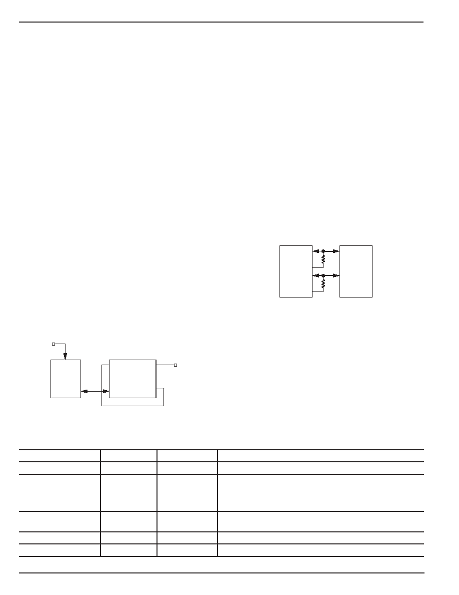
Non-Multiplexed Bus
In order to save pin count for the USB logic controller
interface, the MIC2551 was designed with V
P and VM as bi-
directional pins. To interface the MIC2551 with a non-multi-
plexed data bus, resistors can be used for low cost isolation
as shown in Figure 8.
VPO
VP
VM
VMO
USB Logic
Controller
(SIE)
MIC2551
VP
VM
10k
Figure 8. MIC2551 Interface to
Non-Multiplexed Data Bus
Configuration Mode
VBUS/VTRM
VIF
Notes
Normal
Connected
Normal supply configuration and operation.
Disconnect
Open
Connected
VP/VM are HIGH outputs, RCV is LOW.
(D+/D– sharing)
With OE# = 0 and SUS = 1, data lines may be driven with
external devices up to 3.6V.
With D+, D– floating, I
IF draws less than 1A.
Disconnect
Ground
Connected
VP/VM are HIGH outputs, RCV is LOW.
With D+, D– floating, I
IF draws less than 1A.
Disable Mode
Connected
Open
Logic controlled inputs pins are Hi-Z.
Prohibited
Connected
Ground
Prohibited condition.
Table 3. Power Supply Configuration
相关PDF资料 |
PDF描述 |
|---|---|
| MIC2551AYML25 TR | IC USB TRANSCEIVER 14-MLF |
| MIC2555-1BML TR | IC TXRX UTG USB BUS UNIV 24MLF |
| MIC3000BML TR | IC TXRX OPTICAL MANAGEMENT 24MLF |
| MIC3001BML TR | IC FOM MANAGEMENT W/CALIBR 24MLF |
| MIC74BQS TR | IC I/O EXPANDER I2C 8B 16QSOP |
相关代理商/技术参数 |
参数描述 |
|---|---|
| MIC2551AYML | 制造商:Rochester Electronics LLC 功能描述: 制造商:RF Micro Devices Inc 功能描述: |
| MIC2551AYML TR | 功能描述:USB 接口集成电路 USB Transceiver - Lead Free RoHS:否 制造商:Cypress Semiconductor 产品:USB 2.0 数据速率: 接口类型:SPI 工作电源电压:3.15 V to 3.45 V 工作电源电流: 最大工作温度:+ 85 C 安装风格:SMD/SMT 封装 / 箱体:WLCSP-20 |
| MIC2551AYML25 | 制造商:Rochester Electronics LLC 功能描述: 制造商:RF Micro Devices Inc 功能描述: 制造商:Micrel Inc 功能描述: |
| MIC2551AYML25 TR | 功能描述:USB 接口集成电路 USB Transceiver - Lead Free RoHS:否 制造商:Cypress Semiconductor 产品:USB 2.0 数据速率: 接口类型:SPI 工作电源电压:3.15 V to 3.45 V 工作电源电流: 最大工作温度:+ 85 C 安装风格:SMD/SMT 封装 / 箱体:WLCSP-20 |
| MIC2551AYML25-TR | 功能描述:1/1 Transceiver Half USB 2.0 14-MLF? (2.5x2.5) 制造商:microchip technology 系列:- 包装:剪切带(CT) 零件状态:停产 类型:收发器 协议:USB 2.0 驱动器/接收器数:1/1 双工:半 接收器滞后:200mV 数据速率:12Mbps 电压 - 电源:4 V ~ 5.25 V 工作温度:-40°C ~ 85°C 安装类型:表面贴装 封装/外壳:14-VFQFN 裸露焊盘,14-MLF? 供应商器件封装:14-MLF?(2.5x2.5) 标准包装:1 |
发布紧急采购,3分钟左右您将得到回复。