- 您现在的位置:买卖IC网 > PDF目录13080 > MIC9131YM TR (Micrel Inc)IC CTRLR DC-DC PWM HV HS 16-SOIC PDF资料下载
参数资料
| 型号: | MIC9131YM TR |
| 厂商: | Micrel Inc |
| 文件页数: | 16/19页 |
| 文件大小: | 0K |
| 描述: | IC CTRLR DC-DC PWM HV HS 16-SOIC |
| 标准包装: | 2,500 |
| 应用: | 控制器,电信 |
| 输入电压: | 9 V ~ 18 V |
| 输出数: | 1 |
| 输出电压: | 4.7 V ~ 5 V |
| 工作温度: | -40°C ~ 125°C |
| 安装类型: | 表面贴装 |
| 封装/外壳: | 16-SOIC(0.154",3.90mm 宽) |
| 供应商设备封装: | 16-SOIC |
| 包装: | 带卷 (TR) |
| 其它名称: | MIC9131YMTR MIC9131YMTR-ND |
�� �
�
�MIC9131�
�If� the� current� sense� transformer� were� not� used,� the� sense�
�resistor� would� dissipate� 1.7� watts.�
�Micrel,� Inc.�
�secondary� winding� inductance� for� the� ?yback�
�topology)�
�R� SENSE� =� =�
�V� SENSE�
�I� SENSE�
�0� .� 82�
�5�
�=� 0� .� 164� ?�
�M2� is� the� inductor� current� downslope�
�For� a� boost� topology,� the� inductor� downslope� is:�
�R1�
�di� V� ?� V� IN� +� V� D�
�M� 2� =� =� OUT�
�M� 2� REFLECTED� =� M� 2� �
�P� DISS� =� I� RMS� 2� � R� SENSE� =� 3� .� 25� 2� � 0� .� 164� =� 1� .� 7� W�
�Slope� Compensation�
�Power� supplies� using� peak� current� mode� control� techniques�
�require� slope� compensation� when� they� are� operating� in�
�continuous� mode� and� have� a� duty� cycle� greater� than� 50%.�
�Without� slope� compensation,� the� duty� cycle� of� the� power� sup-�
�ply� will� alternate� wide� and� narrow� pulses� commonly� referred�
�to� as� subharmonic� oscillations.� Even� though� the� MIC9131�
�operates� below� a� 50%� duty� cycle,� slope� compensation� adds�
�the� bene?ts� of� improved� transient� response� and� greater�
�noise� immunity� in� the� current� sense� loop� (especially� when�
�the� current� ramp� is� shallow).� Slope� compensation� can� be�
�implemented� by� adding� an� optimum� 1/2� of� the� inductor� cur-�
�rent� downslope,� re?ected� back� to� the� current� sense� input.� In�
�real� world� applications,� 2/3� of� the� inductor� current� downslope�
�is� used� to� allow� for� component� tolerances.�
�Slope� compensation� at� the� ISNS� input� may� be� implemented�
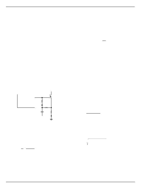
�by� using� a� resistor� and� capacitor� as� shown� in� Figure� 12.� The�
�rectangular� waveshape� of� the� gate� drive� output� is� integrated�
�by� the� resistor/capacitor� ?lter,� which� results� in� a� ramp� used�
�for� the� slope� compensation� signal.� When� the� gate� drive� and�
�the� current� signal� at� the� sense� resistor� goes� low,� the� capaci-�
�tor� is� discharged� to� 0V.�
�Gate� Drive�
�(pin� 16)�
�MIC9131� R2�
�I� SNS�
�(pin� 14)�
�dt� L�
�In� a� transformer� isolated� topology,� the� downslope� must� be�
�re?ected� back� to� the� primary� by� the� turns� ratio� of� the� trans-�
�former.� The� re?ected� downslope� is:�
�Ns�
�Np�
�where� :� Ns/Np� is� the� turns� ratio� of� the� secondary� winding�
�to� the� primary� winding.�
�M2� REFLECTED� is� the� inductor� curent� downslope�
�re?ected� to� the� secondary� side� of� the� current�
�sense� transformer.�
�The� re?ected� downslope� is� multiplied� by� the� current� sense�
�resistor� to� obtain� the� downslope� at� the� current� sense� input�
�pin� (ISNS).�
�I� SNS� _� SLOPE� =� M� 2� REFLECTED� � R� S�
�where� Rs� is� the� value� of� the� current� sense� resistor.�
�The� required� downslope� of� the� compensation� ramp� at� the�
�ISNS� input� is:�
�M� 3� =� I� SNS� _� SLOPE� � 0� .� 67�
�R1� is� know� if� a� value� for� the� resistor� between� the� current�
�sense� resistor� and� the� Isns� pin,� has� already� been� selected.�
�If� not� chose� a� value� of� 1k,� which� will� minimize� any� offset�
�and� signal� degradation� at� the� ISNS� pin.� Select� a� value� of�
�C1� to� minimize� signal� degradation� from� the� cutoff� frequency�
�of� R1/C1.� The� bandwidth� should� be� at� least� six� times� the�
�switching� frequency.�
�C1�
�R� SENSE�
�C� 1� =�
�1�
�2� ×� π� ×� f� S� ×� R� 1�
�M� 3� =� V� GATE_DRIVE� �
��
�V� GATE� _� DRIVE� � R� 1�
�M� 3� � C� 1�
�di� V� +� V� D�
�M� 2� =� =� O�
�Figure� 12�
�The� procedure� outlined� below� demonstrates� how� to� calculate�
�the� component� values.�
�Compute� the� inductor� current� downslope� as� seen� at� the� cur-�
�rent� sense� input.�
�For� a� ?yback,� buck� or� forward� mode� topology� the�
�inductor� downslope� is� equal� to:�
�dt� L�
�where� :�
�V� O� is� the� output� voltage�
�V� D� is� the� forward� voltage� drop� of� the� recti?er� diode�
�L� is� the� inductance� of� the� output� inductor� (or� the�
�where:� f� S� is� the� switching� frequency� of� the� power�
�supply� (not� the� oscillator� frequency)�
�The� slope� of� the� generated� compensation� ramp� is:�
�R1� 1�
�R2� +� R1� R2� � C1�
�Solving� for� R2� and� assuming� R2� is� much� greater� than� R1.�
�R� 2� =�
�where:� V� GATE_DRIVE� is� the� amplitude� of� the� gate�
�drive� waveform�
�M9999-080206�
�16�
�August� 2006�
�相关PDF资料 |
PDF描述 |
|---|---|
| SPX29302T5-L | IC REG LDO ADJ 3A TO263-5 |
| VI-JWJ-EZ-B1 | CONVERTER MOD DC/DC 36V 25W |
| MIC9130YQS TR | IC CTRLR DC-DC PWM HV HS 16-QSOP |
| HSC25DRTI-S13 | CONN EDGECARD 50POS .100 EXTEND |
| EBC43DREI-S13 | CONN EDGECARD 86POS .100 EXTEND |
相关代理商/技术参数 |
参数描述 |
|---|---|
| MIC9131YQS | 功能描述:电流型 PWM 控制器 SO-16 High Vin Telecom DC/DC PWM Control IC (Lead Free) RoHS:否 制造商:Texas Instruments 开关频率:27 KHz 上升时间: 下降时间: 工作电源电压:6 V to 15 V 工作电源电流:1.5 mA 输出端数量:1 最大工作温度:+ 105 C 安装风格:SMD/SMT 封装 / 箱体:TSSOP-14 |
| MIC9131YQS TR | 功能描述:电流型 PWM 控制器 SO-16 High Vin Telecom DC/DC PWM Control IC (Lead Free) RoHS:否 制造商:Texas Instruments 开关频率:27 KHz 上升时间: 下降时间: 工作电源电压:6 V to 15 V 工作电源电流:1.5 mA 输出端数量:1 最大工作温度:+ 105 C 安装风格:SMD/SMT 封装 / 箱体:TSSOP-14 |
| MIC913BM5 | 制造商:Rochester Electronics LLC 功能描述:- Bulk |
| MIC913BM5 TR | 功能描述:IC OPAMP 350MHZ HS LP SOT23-5 RoHS:否 类别:集成电路 (IC) >> Linear - Amplifiers - Instrumentation 系列:- 标准包装:2,500 系列:- 放大器类型:通用 电路数:1 输出类型:满摆幅 转换速率:0.11 V/µs 增益带宽积:350kHz -3db带宽:- 电流 - 输入偏压:4nA 电压 - 输入偏移:20µV 电流 - 电源:260µA 电流 - 输出 / 通道:20mA 电压 - 电源,单路/双路(±):2.7 V ~ 36 V,±1.35 V ~ 18 V 工作温度:-40°C ~ 85°C 安装类型:表面贴装 封装/外壳:8-SOIC(0.154",3.90mm 宽) 供应商设备封装:8-SO 包装:带卷 (TR) |
| MIC913YM5 TR | 功能描述:运算放大器 - 运放 350MHz, 4.2mA High Speed Op Amp RoHS:否 制造商:STMicroelectronics 通道数量:4 共模抑制比(最小值):63 dB 输入补偿电压:1 mV 输入偏流(最大值):10 pA 工作电源电压:2.7 V to 5.5 V 安装风格:SMD/SMT 封装 / 箱体:QFN-16 转换速度:0.89 V/us 关闭:No 输出电流:55 mA 最大工作温度:+ 125 C 封装:Reel |
发布紧急采购,3分钟左右您将得到回复。