- 您现在的位置:买卖IC网 > PDF目录18782 > MICRF002YM (Micrel Inc)IC ASK RCVR RF/IF SHUTDWN 16SOIC PDF资料下载
参数资料
| 型号: | MICRF002YM |
| 厂商: | Micrel Inc |
| 文件页数: | 12/17页 |
| 文件大小: | 0K |
| 描述: | IC ASK RCVR RF/IF SHUTDWN 16SOIC |
| 标准包装: | 48 |
| 系列: | QwikRadio® |
| 频率: | 300MHz ~ 440MHz |
| 灵敏度: | -95dBm |
| 数据传输率 - 最大: | 10 kbps |
| 调制或协议: | ASK,OOK |
| 应用: | RKE |
| 电流 - 接收: | 2.2mA |
| 数据接口: | PCB,表面贴装 |
| 天线连接器: | PCB,表面贴装 |
| 特点: | 自动调谐 |
| 电源电压: | 4.75 V ~ 5.5 V |
| 工作温度: | -40°C ~ 85°C |
| 封装/外壳: | 16-SOIC(0.154",3.90mm 宽) |
| 供应商设备封装: | 16-SOIC |
| 包装: | 管件 |
| 产品目录页面: | 571 (CN2011-ZH PDF) |
| 其它名称: | 576-1332 |
�� �
�
�Micrel,� Inc.�
�Power� Supply� Bypass� Capacitors�
�V� DDBB� and� V� DDRF� should� be� connected� together� directly� at�
�the� IC� pins.� Supply� bypass� capacitors� are� strongly�
�recommended.� They� should� be� connected� to� V� DDBB� and�
�V� DDRF� and� should� have� the� shortest� possible� lead� lengths.�
�For� best� performance,� connect� V� SSRF� to� V� SSBB� at� the� power�
�supply� only� (that� is,� keep� V� SSBB� currents� from� flowing�
�through� the� V� SSRF� return� path).�
�Increasing� Selectivity� with� an� Optional� BandPass�
�Filter�
�For� applications� located� in� high� ambient� noise�
�environments,� a� fixed� value� band-pass� network� may� be�
�connected� between� the� ANT� pin� and� V� SSRF� to� provide�
�additional� receive� selectivity� and� input� overload� protection.�
�A� minimum� input� configuration� is� included� in� Figure� 7� it�
�provides� some� filtering� and� necessary� overload� protection.�
�Data� Squelching�
�During� quiet� periods� (no� signal)� the� data� output� (DO� pin)�
�transitions� randomly� with� noise.� Most� decoders� can�
�discriminate� between� this� random� noise� and� actual� data� but�
�for� some� system� it� does� present� a� problem.� There� are� three�
�possible� approaches� to� reducing� this� output� noise:�
�1.� Analog� squelch� to� raise� the� demodulator� threshold�
�2.� Digital� squelch� to� disable� the� output� when� data� is�
�not� present�
�3.� Output� filter� to� filter� the� (high� frequency)� noise�
�glitches� on� the� data� output� pin.�
�The� simplest� solution� is� add� analog� squelch� by� introducing�
�MICRF002/RF022�
�reference� oscillator� and� is� 1/256� the� reference� oscillator�
�frequency.� For� example:�
�f� T� =� 6.4MHz�
�f� S� =� f� T� /256� =� 25kHz�
�P� S� =� 1/f� S� =� 0.04ms�
�128� counts� x� 0.04ms� =� 5.12ms�
�where:�
�f� T� =� reference� oscillator� frequency�
�f� S� =� system� clock� frequency�
�P� S� =� system� clock� period�
�The� Wake-Up� counter� will� reset� immediately� after� a�
�detected� RF� carrier� drops.� The� duration� of� the� Wake-Up�
�signal� output� is� then� determined� by� the� required� wake� up�
�time� plus� an� additional� RF� carrier� on� time� interval� to� create�
�a� wake� up� pulse� output.�
�WAKEB� Output� Pulse� Time� =� T� WAKE� +� Additional�
�RF� Carrier� On� Time�
�For� designers� who� wish� to� use� the� wakeup� function� while�
�squelching� the� output,� a� positive� squelching� offset� voltage�
�must� be� used.� This� simply� requires� that� the� squelch� resistor�
�be� connected� to� a� voltage� more� positive� than� the� quiescent�
�voltage� on� the� C� TH� pin� so� that� the� data� output� is� low� in�
�absence� of� a� transmission.�
�I/O� Pin� Interface� Circuitry�
�Interface� circuitry� for� the� various� I/O� pins� of� the� MICRF002�
�are� diagrammed� in� Figures� 1� through� 6.� The� ESD�
�protection� diodes� at� all� input� and� output� pins� are� not� shown.�
�a� small� offset,� or� squelch� voltage,� on� the� C� TH� pin� so� that�
�noise� does� not� trigger� the� internal� comparator.� Usually�
�20mV� to� 30mV� is� sufficient,� and� may� be� achieved� by�
�C� TH� Pin�
�VDDBB�
�connecting� a� several-megohm� resistor� from� the� C� TH� pin� to�
�either� V� SS� or� V� DD� ,� depending� on� the� desired� offset� polarity.�
�Since� the� MICRF002� has� receiver� AGC� noise� at� the�
�internal� comparator� input� is� always� the� same,� set� by� the�
�AGC.� The� squelch� offset� requirement� does� not� change� as�
�Demodulator�
�Signal�
�2.85Vdc�
�PHI2B�
�PHI1B�
�CTH�
�the� local� noise� strength� changes� from� installation� to�
�installation.� Introducing� squelch� will� reduce� sensitivity� and�
�also� reduce� range.� Only� introduce� an� amount� of� offset�
�VSSBB�
�PHI2�
�VSSBB�
�PHI1�
�sufficient� to� quiet� the� output.� Typical� squelch� resistor� values�
�range� from� 6.8M� ?� to� 10M� ?� .�
�Wake-Up� Function�
�The� WAKEB� output� signal� can� be� used� to� reduce� system�
�power� consumption� by� enabling� the� rest� of� a� system� when�
�an� RF� signal� is� present.� The� WAKEB� is� an� output� logic�
�signal� which� goes� active� low� when� the� IC� detects� a�
�constant� RF� carrier.� The� wake-up� function� is� unavailable�
�when� the� IC� is� in� shutdown� mode.�
�To� activate� the� Wake-Up� function,� a� received� constant� RF�
�carrier� must� be� present� for� 128� counts� or� the� internal�
�system� clock.� The� internal� system� clock� is� derived� from� the�
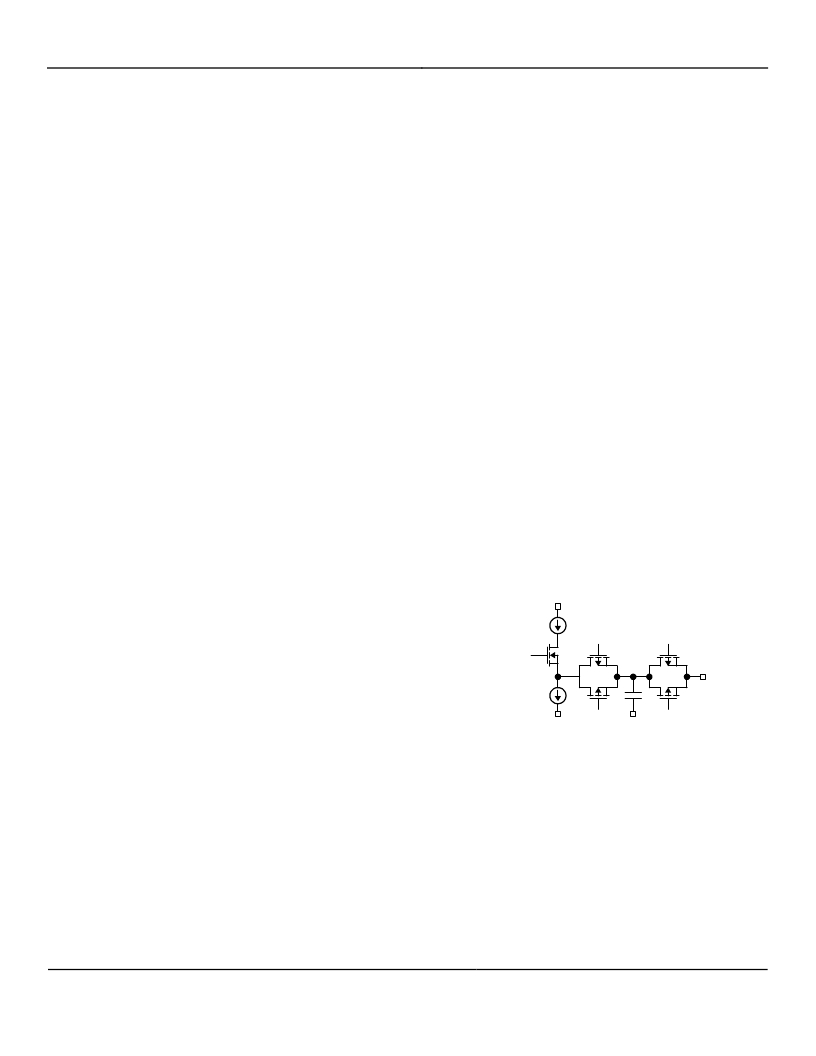
�Figure� 2.� CTH� Pin�
�Figure� 2� illustrates� the� C� TH� pin� interface� circuit.� The� C� TH� pin�
�is� driven� from� a� P-channel� MOSFET� source-follower� with�
�approximately� 10� μ� A� of� bias.� Transmission� gates� TG1� and�
�TG2� isolate� the� 6.9pF� capacitor.� Internal� control� signals�
�PHI1/PHI2� are� related� in� a� manner� such� that� the�
�impedance� across� the� transmission� gates� looks� like� a�
�“resistance”� of� approximately� 100k� ?� .� The� dc� potential� at�
�the� C� TH� pin� is� approximately� 1.6V�
�July� 2008�
�12�
�M9999-070808�
�相关PDF资料 |
PDF描述 |
|---|---|
| 6267 | KIT REPLACE ACCESS OSCILLOSCOPE |
| MICRF010YM | IC RCVR UHF 300-440MHZ 8-SOIC |
| IXTY1R6N50D2 | MOSFET N-CH 500V 1.6A DPAK |
| IXTA7N60P | MOSFET N-CH 600V 7A D2-PAK |
| MICRF213AYQS | IC RX 3.3V 300-350 MHZ 16-QSOP |
相关代理商/技术参数 |
参数描述 |
|---|---|
| MICRF002YM TR | 功能描述:射频接收器 300-440MHz RF Receiver With Shutdown( Lead Free) RoHS:否 制造商:Skyworks Solutions, Inc. 类型:GPS Receiver 封装 / 箱体:QFN-24 工作频率:4.092 MHz 工作电源电压:3.3 V 封装:Reel |
| MICRF003 | 制造商:MICREL 制造商全称:Micrel Semiconductor 功能描述:QwikRadiotm 900 MHz UHF Receiver Preliminary Information |
| MICRF003BM | 功能描述:IC RECEIVER UHF 900MHZ 16-SOIC RoHS:否 类别:RF/IF 和 RFID >> RF 接收器 系列:- 产品培训模块:Lead (SnPb) Finish for COTS 产品变化通告:Product Discontinuation 09/Jan/2012 标准包装:50 系列:* 频率:850MHz ~ 2.175GHz 灵敏度:- 数据传输率 - 最大:- 调制或协议:- 应用:* 电流 - 接收:* 数据接口:PCB,表面贴装 存储容量:- 天线连接器:PCB,表面贴装 特点:- 电源电压:4.75 V ~ 5.25 V 工作温度:0°C ~ 85°C 封装/外壳:40-WFQFN 裸露焊盘 供应商设备封装:40-TQFN-EP(6x6) 包装:托盘 |
| MICRF003BM TR | 功能描述:IC RECEIVER UHF 900MHZ 16-SOIC RoHS:否 类别:RF/IF 和 RFID >> RF 接收器 系列:- 产品培训模块:Lead (SnPb) Finish for COTS 产品变化通告:Product Discontinuation 09/Jan/2012 标准包装:50 系列:* 频率:850MHz ~ 2.175GHz 灵敏度:- 数据传输率 - 最大:- 调制或协议:- 应用:* 电流 - 接收:* 数据接口:PCB,表面贴装 存储容量:- 天线连接器:PCB,表面贴装 特点:- 电源电压:4.75 V ~ 5.25 V 工作温度:0°C ~ 85°C 封装/外壳:40-WFQFN 裸露焊盘 供应商设备封装:40-TQFN-EP(6x6) 包装:托盘 |
| MICRF003YM | 功能描述:IC RECEIVER UHF 900MHZ 16-SOIC RoHS:是 类别:RF/IF 和 RFID >> RF 接收器 系列:- 产品培训模块:Lead (SnPb) Finish for COTS 产品变化通告:Product Discontinuation 09/Jan/2012 标准包装:50 系列:* 频率:850MHz ~ 2.175GHz 灵敏度:- 数据传输率 - 最大:- 调制或协议:- 应用:* 电流 - 接收:* 数据接口:PCB,表面贴装 存储容量:- 天线连接器:PCB,表面贴装 特点:- 电源电压:4.75 V ~ 5.25 V 工作温度:0°C ~ 85°C 封装/外壳:40-WFQFN 裸露焊盘 供应商设备封装:40-TQFN-EP(6x6) 包装:托盘 |
发布紧急采购,3分钟左右您将得到回复。