- 您现在的位置:买卖IC网 > PDF目录45328 > MK2049-02SI 51.84 MHz, OTHER CLOCK GENERATOR, PDSO20 PDF资料下载
参数资料
| 型号: | MK2049-02SI |
| 元件分类: | 时钟产生/分配 |
| 英文描述: | 51.84 MHz, OTHER CLOCK GENERATOR, PDSO20 |
| 封装: | 0.300 INCH, SOIC-20 |
| 文件页数: | 10/11页 |
| 文件大小: | 136K |
| 代理商: | MK2049-02SI |
MK2049-02/03
Communications Clock PLLs
MDS 2049-02/03 C
8
Revision 091801
Integrated Circuit Systems, Inc. 525 Race Street San Jose CA 95126 (408)295-9800tel www.icst.com
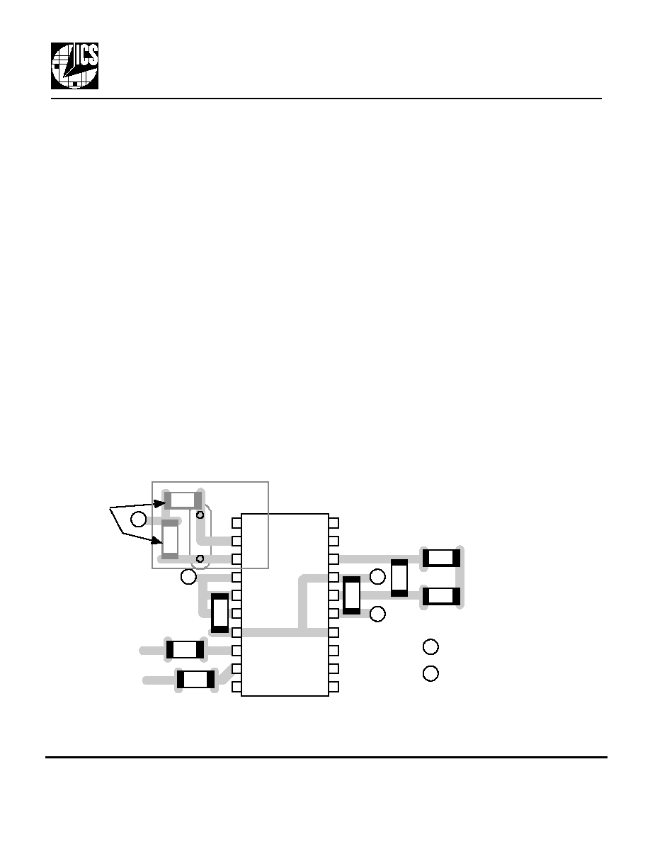
PC Board Layout
=connect to VDD
=connect to GND
V
G
1
16
2
3
4
15
14
13
5
6
8
12
11
10
9
18
20
cap
resist.
cap
G
V
19
17
V
cap
resist.
cap
LAYOUT AND EXTERNAL COMPONENTS
A proper board layout is critical to the successful use of the MK2049. In particular, the CAP1 and CAP2 pins are very
sensitive to noise and leakage (CAP2 at pin 18 is the most sensitive). Traces must be as short as possible and the two
capacitors and resistor must be mounted next to the device as shown below. The capacitor shown between pins 15
and 17, and the one between pins 5 and 7 are the power supply decoupling capacitors. The high frequency output
clocks on pins 8 and 9 should have a series termination of 33
connected close to the pin. Additional improvements
will come from keeping all components on the same side of the board, minimizing vias through other signal layers, and
routing other signals away from the MK2049.
You may also refer to MAN05 for additional suggestions on layout of
the crystal section.
The crystal traces should include pads for small capacitors from X1 and X2 to ground; these are used to adjust the
stray capacitance of the board to match the crystal load capacitance. The typical telecom reference frequency is
accurate to much less than 1 ppm, so the MK2049 may lock and run properly even if the board capacitance is not
adjusted with these fixed capacitors. However, ICS MicroClock recommends that the adjustment capacitors be
included to minimize the effects of variation in individual crystals, temperature, and aging. The value of these
capacitors (typically 0-4 pF) is determined once for a given board layout, using the procedure described in the section
titled “Determining the Crystal Frequency Adjustment Capacitors”.
The MK2049-02/03 require a minimum number of external components for proper operation. Decoupling capacitors
of 0.01F must be connected between VDD and GND pins close to the chip (especially pins 4 and 7, 15 and 17),
and 33
terminating resistors should be used on clock outputs with traces longer than 1 inch (assuming 50
traces).
Figure 3. Typical MK2049-02/03 Layout
7
cap
G
Optional;
see text
Cutout in ground and power plane.
Route all traces away from this area.
相关PDF资料 |
PDF描述 |
|---|---|
| MK2049-11SITR | 56 MHz, OTHER CLOCK GENERATOR, PDSO20 |
| MK2049-11SITRLF | 56 MHz, OTHER CLOCK GENERATOR, PDSO20 |
| MK2049-11SITRLF | 56 MHz, OTHER CLOCK GENERATOR, PDSO20 |
| MK2049-11SI | 56 MHz, OTHER CLOCK GENERATOR, PDSO20 |
| MK2049-45ASI | 125 MHz, OTHER CLOCK GENERATOR, PDSO20 |
相关代理商/技术参数 |
参数描述 |
|---|---|
| MK2049-02SITR | 制造商:ICS 制造商全称:ICS 功能描述:Communications Clock PLLs |
| MK2049-02STR | 制造商:ICS 制造商全称:ICS 功能描述:Communications Clock PLLs |
| MK2049-03S | 制造商:MICROCLOCK 功能描述: |
| MK2049-03SI | 制造商:ICS 制造商全称:ICS 功能描述:Communications Clock PLLs |
| MK2049-03SITR | 制造商:ICS 制造商全称:ICS 功能描述:Communications Clock PLLs |
发布紧急采购,3分钟左右您将得到回复。