- 您现在的位置:买卖IC网 > PDF目录9184 > MK2059-01SILF (IDT, Integrated Device Technology Inc)IC VCXO CLK JITTER ATTEN 20-SOIC PDF资料下载
参数资料
| 型号: | MK2059-01SILF |
| 厂商: | IDT, Integrated Device Technology Inc |
| 文件页数: | 4/11页 |
| 文件大小: | 0K |
| 描述: | IC VCXO CLK JITTER ATTEN 20-SOIC |
| 标准包装: | 37 |
| 类型: | 时钟频率变换器 |
| PLL: | 是 |
| 输入: | LVCMOS |
| 输出: | LVCMOS |
| 电路数: | 1 |
| 比率 - 输入:输出: | 2:1 |
| 差分 - 输入:输出: | 无/无 |
| 频率 - 最大: | 25.92MHz |
| 除法器/乘法器: | 是/无 |
| 电源电压: | 3.15 V ~ 3.45 V |
| 工作温度: | -40°C ~ 85°C |
| 安装类型: | 表面贴装 |
| 封装/外壳: | 20-SOIC(0.295",7.50mm 宽) |
| 供应商设备封装: | 20-SOIC |
| 包装: | 管件 |
| 其它名称: | 800-2263 MK2059-01SILF-ND |
MK2059-01
VCXO-BASED FRAME CLOCK FREQUENCY TRANSLATOR
VCXO AND SYNTHESIZER
IDT VCXO-BASED FRAME CLOCK FREQUENCY TRANSLATOR
2
MK2059-01
REV H 051310
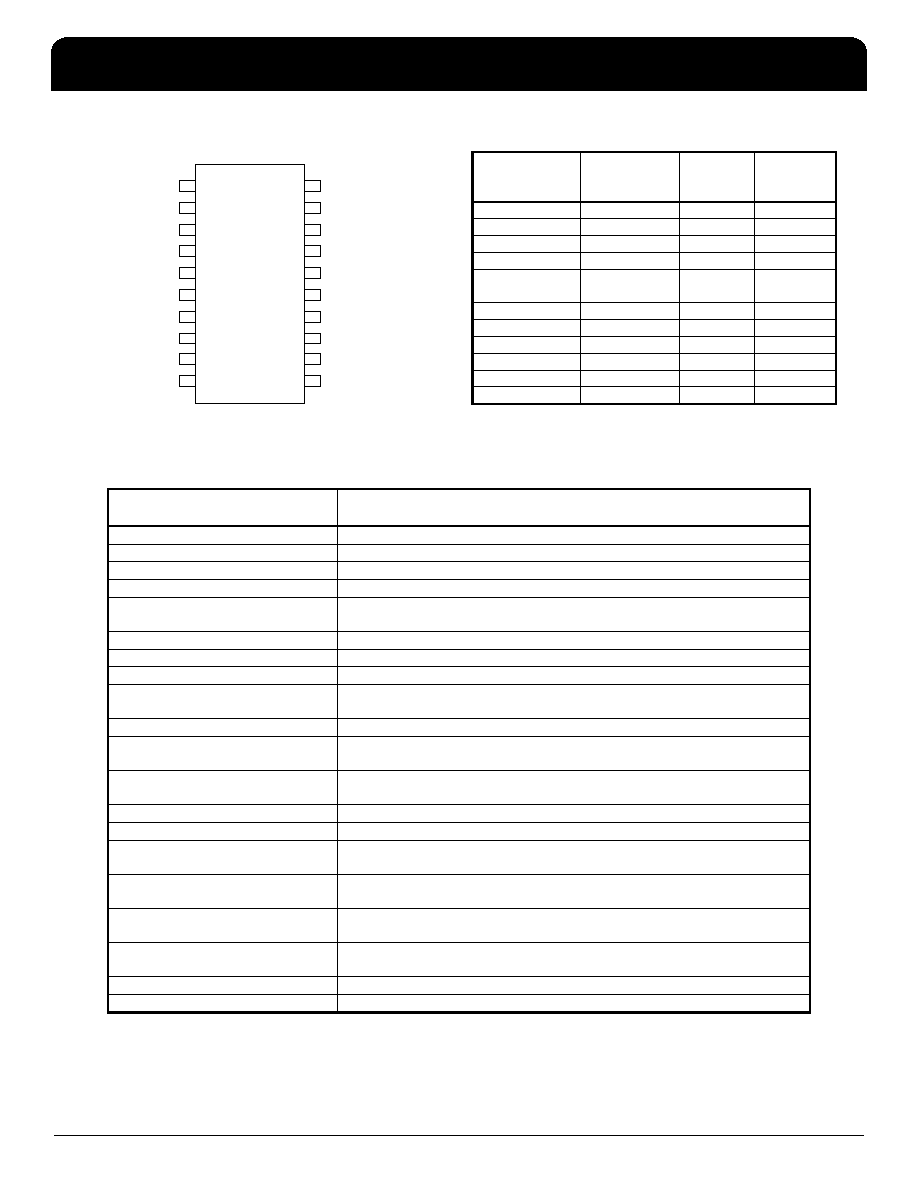
Pin Assignment
20 pin 300 mil SOIC
Output Clock Selection Table
Note: For SEL input pin programming:
0 = GND, 1 = VDD, M = Floating
Pin Descriptions
16
1
15
2
14
X1
X 2
3
13
VD D
4
12
VD D
GN D
5
11
VD D
6
ISEL
7
VIN
8
GN D
IC L K 1
IC L K 2
SEL0
GN D
CL K
GN D
NC
9
10
CH G P
SEL1
IS E T
SEL2
20
19
18
17
Input
SEL2
SEL1
SEL0
Output
Clock
(MHz)
Crystal
Used (MHz)
8 kHz
0
1.544
24.704
8 kHz
0
1
2.048
24.576
8 kHz
0
1
0
16.384
8 kHz
0
1
17.664
8 kHz
M
0
18.528
8 kHz
M
0
1
20.00
8 kHz
M
1
0
25.00
8 kHz
M
1
25.92
8 kHz
1
0
19.44
8 kHz
1
0
1
20.48
8 kHz
1
0
24.704
8 kHz
1
24.576
Pin
Number
Pin
Name
Pin
Type
Pin Description
1
X1
-
Crystal Input. Connect this pin to the specified crystal.
2
VDD
Power
Power Supply. Connect to +3.3V.
3
VDD
Power
Power Supply. Connect to +3.3V.
4
VDD
Power
Power Supply. Connect to +3.3V.
5
VIN
Input
VCXO Control Voltage Input. Connect this pin to CHGP pin and the external
loop filter as shown in this data sheet.
6
GND
Power
Connect to ground
7
GND
Power
Connect to ground
8
GND
Power
Connect to ground
9
CHGP
Output
Charge Pump Output. Connect this pin to the external loop filter and to pin
VIN.
10
ISET
-
Charge pump current setting node, connection for setting resistor.
11
SEL2
Input
Output Frequency Selection Pin 2. Determines output frequency as per table
above. Internally biased to VDD/2.
12
SEL1
Input
Output Frequency Selection Pin 1. Determines output frequency as per table
above. Internal pull-up.
13
NC
Input
No Internal Connection.
14
CLK
Output
Clock Output
15
SEL0
Input
Output Frequency Selection Pin 0. Determines output frequency as per table
above. Internal pull-up.
16
ICLK2
Input
Input Clock Connection 2. Connect an input reference clock to this pin. If
unused, connect to ground.
17
ICLK1
Input
Input Clock Connection 1. Connect an input reference clock to this pin. If
unused, connect to ground.
18
ISEL
Input
Input Selection. Used to select which reference input clock is active. Low input
level selects ICLK1, high input level selects ICLK2. Internal pull-up.
19
GND
Power
Connect to ground.
20
X2
-
Crystal Output. Connect this pin to the specified crystal.
相关PDF资料 |
PDF描述 |
|---|---|
| VI-B4W-MW-B1 | CONVERTER MOD DC/DC 5.5V 100W |
| VI-B4V-MW-B1 | CONVERTER MOD DC/DC 5.8V 100W |
| MS27468E25F35SA | CONN RCPT 128POS JAM NUT W/SCKT |
| MS27656T17B6P | CONN RCPT 6POS WALL MNT W/PINS |
| VI-B54-MW-B1 | CONVERTER MOD DC/DC 48V 100W |
相关代理商/技术参数 |
参数描述 |
|---|---|
| MK2059-01SILFTR | 功能描述:时钟发生器及支持产品 VCXO-BASED FRAME CLK FREQUENCY TRANSLATOR RoHS:否 制造商:Silicon Labs 类型:Clock Generators 最大输入频率:14.318 MHz 最大输出频率:166 MHz 输出端数量:16 占空比 - 最大:55 % 工作电源电压:3.3 V 工作电源电流:1 mA 最大工作温度:+ 85 C 安装风格:SMD/SMT 封装 / 箱体:QFN-56 |
| MK2059-01SITR | 功能描述:IC VCXO CLK JITTER ATTEN 20-SOIC RoHS:否 类别:集成电路 (IC) >> 时钟/计时 - 时钟发生器,PLL,频率合成器 系列:- 标准包装:39 系列:- 类型:* PLL:带旁路 输入:时钟 输出:时钟 电路数:1 比率 - 输入:输出:1:10 差分 - 输入:输出:是/是 频率 - 最大:170MHz 除法器/乘法器:无/无 电源电压:2.375 V ~ 3.465 V 工作温度:0°C ~ 70°C 安装类型:* 封装/外壳:* 供应商设备封装:* 包装:* |
| MK2069-01 | 制造商:ICS 制造商全称:ICS 功能描述:VCXO-Based Line Card Clock Synchronizer |
| MK2069-01GI | 功能描述:IC VCXO CLK SYNCHRONIZER 56TSSOP RoHS:否 类别:集成电路 (IC) >> 时钟/计时 - 时钟发生器,PLL,频率合成器 系列:- 标准包装:39 系列:- 类型:* PLL:带旁路 输入:时钟 输出:时钟 电路数:1 比率 - 输入:输出:1:10 差分 - 输入:输出:是/是 频率 - 最大:170MHz 除法器/乘法器:无/无 电源电压:2.375 V ~ 3.465 V 工作温度:0°C ~ 70°C 安装类型:* 封装/外壳:* 供应商设备封装:* 包装:* |
| MK2069-01GILF | 功能描述:时钟合成器/抖动清除器 VCXO-BASED LINE CARD CLOCK SYNCHRONIZER RoHS:否 制造商:Skyworks Solutions, Inc. 输出端数量: 输出电平: 最大输出频率: 输入电平: 最大输入频率:6.1 GHz 电源电压-最大:3.3 V 电源电压-最小:2.7 V 封装 / 箱体:TSSOP-28 封装:Reel |
发布紧急采购,3分钟左右您将得到回复。