- 您现在的位置:买卖IC网 > PDF目录9184 > MK2059-01SILF (IDT, Integrated Device Technology Inc)IC VCXO CLK JITTER ATTEN 20-SOIC PDF资料下载
参数资料
| 型号: | MK2059-01SILF |
| 厂商: | IDT, Integrated Device Technology Inc |
| 文件页数: | 7/11页 |
| 文件大小: | 0K |
| 描述: | IC VCXO CLK JITTER ATTEN 20-SOIC |
| 标准包装: | 37 |
| 类型: | 时钟频率变换器 |
| PLL: | 是 |
| 输入: | LVCMOS |
| 输出: | LVCMOS |
| 电路数: | 1 |
| 比率 - 输入:输出: | 2:1 |
| 差分 - 输入:输出: | 无/无 |
| 频率 - 最大: | 25.92MHz |
| 除法器/乘法器: | 是/无 |
| 电源电压: | 3.15 V ~ 3.45 V |
| 工作温度: | -40°C ~ 85°C |
| 安装类型: | 表面贴装 |
| 封装/外壳: | 20-SOIC(0.295",7.50mm 宽) |
| 供应商设备封装: | 20-SOIC |
| 包装: | 管件 |
| 其它名称: | 800-2263 MK2059-01SILF-ND |
MK2059-01
VCXO-BASED FRAME CLOCK FREQUENCY TRANSLATOR
VCXO AND SYNTHESIZER
IDT VCXO-BASED FRAME CLOCK FREQUENCY TRANSLATOR
5
MK2059-01
REV H 051310
A “normalized” PLL loop bandwidth may be calculated as
follows:
The “normalized” bandwidth equation above does not take
into account the effects of damping factor or the second
pole. However, it does provide a useful approximation of
filter performance.
The loop damping factor is calculated as follows:
Where:
RZ = Value of resistor in loop filter (Ohms)
ICP = Charge pump current (amps)
(refer to Charge Pump Current Table, below)
N = Crystal multiplier shown in the above table
C1 = Value of capacitor C1 in loop filter (Farads)
As a general rule, the following relationship should be
maintained between components C1 and C2 in the loop
filter:
Charge Pump Current Table
found on the IDT web site.
Series Termination Resistor
Clock output traces over one inch should use series
termination. To series terminate a 50
trace (a commonly
used trace impedance), place a 33
resistor in series with
the clock line, as close to the clock output pin as possible.
The nominal impedance of the clock output is 20
. (The
optional series termination resistor is not shown in the
External Component Schematic.)
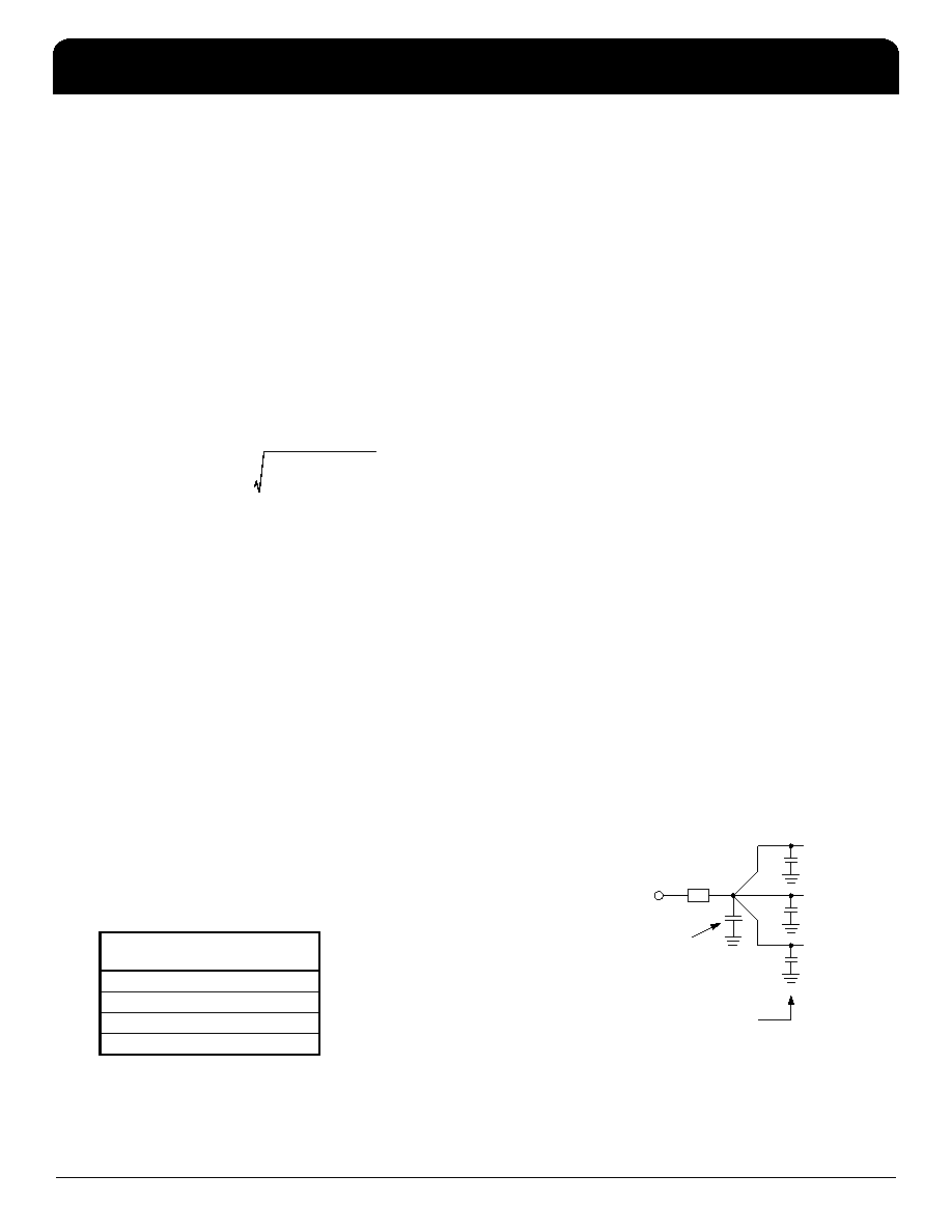
Decoupling Capacitors
As with any high performance mixed-signal IC, the
MK2059-01 must be isolated from system power supply
noise to perform optimally.
Decoupling capacitors of 0.01F must be connected
between each VDD and the PCB ground plane. To further
guard against interfering system supply noise, the
MK2059-01 should use one common connection to the PCB
power plane as shown in the diagram on the next page. The
ferrite bead and bulk capacitor help reduce lower frequency
noise in the supply that can lead to output clock phase
modulation.
Recommended Power Supply Connection for
Optimal Device Performance
RSET
Charge Pump Current
(ICP)
1.4 M
10
A
680 k
20
A
540 k
25
A
120 k
100
A
NBW
RS ICP
×
575
×
N
-----------------------------------------
=
Damping Factor
RS
625
I
CP
×
CS
×
N
-------------------------------------------
×
=
CP
CS
20
------
=
C onnec tion to 3.3V
Pow er Plane
Ferrite
B ead
B ulk D ec oupling C apac itor
(suc h as 1
F Tantalum )
VD D Pin
0.01
F D ecoupling C apacitors
相关PDF资料 |
PDF描述 |
|---|---|
| VI-B4W-MW-B1 | CONVERTER MOD DC/DC 5.5V 100W |
| VI-B4V-MW-B1 | CONVERTER MOD DC/DC 5.8V 100W |
| MS27468E25F35SA | CONN RCPT 128POS JAM NUT W/SCKT |
| MS27656T17B6P | CONN RCPT 6POS WALL MNT W/PINS |
| VI-B54-MW-B1 | CONVERTER MOD DC/DC 48V 100W |
相关代理商/技术参数 |
参数描述 |
|---|---|
| MK2059-01SILFTR | 功能描述:时钟发生器及支持产品 VCXO-BASED FRAME CLK FREQUENCY TRANSLATOR RoHS:否 制造商:Silicon Labs 类型:Clock Generators 最大输入频率:14.318 MHz 最大输出频率:166 MHz 输出端数量:16 占空比 - 最大:55 % 工作电源电压:3.3 V 工作电源电流:1 mA 最大工作温度:+ 85 C 安装风格:SMD/SMT 封装 / 箱体:QFN-56 |
| MK2059-01SITR | 功能描述:IC VCXO CLK JITTER ATTEN 20-SOIC RoHS:否 类别:集成电路 (IC) >> 时钟/计时 - 时钟发生器,PLL,频率合成器 系列:- 标准包装:39 系列:- 类型:* PLL:带旁路 输入:时钟 输出:时钟 电路数:1 比率 - 输入:输出:1:10 差分 - 输入:输出:是/是 频率 - 最大:170MHz 除法器/乘法器:无/无 电源电压:2.375 V ~ 3.465 V 工作温度:0°C ~ 70°C 安装类型:* 封装/外壳:* 供应商设备封装:* 包装:* |
| MK2069-01 | 制造商:ICS 制造商全称:ICS 功能描述:VCXO-Based Line Card Clock Synchronizer |
| MK2069-01GI | 功能描述:IC VCXO CLK SYNCHRONIZER 56TSSOP RoHS:否 类别:集成电路 (IC) >> 时钟/计时 - 时钟发生器,PLL,频率合成器 系列:- 标准包装:39 系列:- 类型:* PLL:带旁路 输入:时钟 输出:时钟 电路数:1 比率 - 输入:输出:1:10 差分 - 输入:输出:是/是 频率 - 最大:170MHz 除法器/乘法器:无/无 电源电压:2.375 V ~ 3.465 V 工作温度:0°C ~ 70°C 安装类型:* 封装/外壳:* 供应商设备封装:* 包装:* |
| MK2069-01GILF | 功能描述:时钟合成器/抖动清除器 VCXO-BASED LINE CARD CLOCK SYNCHRONIZER RoHS:否 制造商:Skyworks Solutions, Inc. 输出端数量: 输出电平: 最大输出频率: 输入电平: 最大输入频率:6.1 GHz 电源电压-最大:3.3 V 电源电压-最小:2.7 V 封装 / 箱体:TSSOP-28 封装:Reel |
发布紧急采购,3分钟左右您将得到回复。