- 您现在的位置:买卖IC网 > PDF目录45328 > MK2069-01GILFTR (INTEGRATED DEVICE TECHNOLOGY INC) 160 MHz, OTHER CLOCK GENERATOR, PDSO56 PDF资料下载
参数资料
| 型号: | MK2069-01GILFTR |
| 厂商: | INTEGRATED DEVICE TECHNOLOGY INC |
| 元件分类: | 时钟产生/分配 |
| 英文描述: | 160 MHz, OTHER CLOCK GENERATOR, PDSO56 |
| 封装: | 6.10 MM, 0.50 MM PITCH, TSSOP-56 |
| 文件页数: | 1/21页 |
| 文件大小: | 211K |
| 代理商: | MK2069-01GILFTR |
DATASHEET
VCXO-BASED LINE CARD CLOCK SYNCHRONIZER
MK2069-01
IDT VCXO-BASED LINE CARD CLOCK SYNCHRONIZER
1
MK2069-01
REV K 051310
Description
The MK2069-01 is a VCXO (Voltage Controlled Crystal
Oscillator) based clock generator that offers system
synchronization, jitter attenuation, and frequency
multiplication or translation. It can accept an unstable, jittery
input clock and provide a de-jittered, low phase noise
output clock at a user determined frequency. The device’s
clock multiplication ratios are user selectable since all major
PLL divider blocks can be configured through device pin
settings. External PLL loop filter components allow tailoring
of the VCXO PLL loop response and therefore the clock
jitter attenuation characteristics.
The MK2069-01 is ideal for line card applications. Its three
input MUX enables selection of the master or slave
(backup) system clocks, as well as a backup local line card
clock. The lock detector (LD) output serves as a clock
status monitor. The clear (CLR) input enables rapid
synchronization to the phase of a newly selected input
clock, while eliminating the generation of extra clock cycles
and wander caused by memory in the PLL feedback divider.
CLR also serves as a temporary holdover function when
kept low.
Features
Input clock frequency of 1 kHz to 170 MHz
Output clock frequency of 500 kHz to 160 MHz
Jitter attenuation of input clock provided by VCXO circuit.
Jitter transfer characteristics user configured through
selection of external loop filter components.
3:1 Input MUX for input reference clocks
PLL lock status output
PLL Clear function allows seamless synchronizing to an
altered input clock phase, virtually eliminating the
generation of wander or extra clock cycles.
VCXO-based clock generation offers very low jitter and
phase noise generation, even with a low frequency or
jittery input clock.
2nd PLL provides translation of VCXO PLL output
(VCLK) to higher or alternate clock frequencies (TCLK).
Device will free-run in the absence of an input clock
based on the VCXO crystal frequency.
56 pin TSSOP package
Single 3.3 V power supply
5 V tolerant inputs on ICLK0 and ICLK1
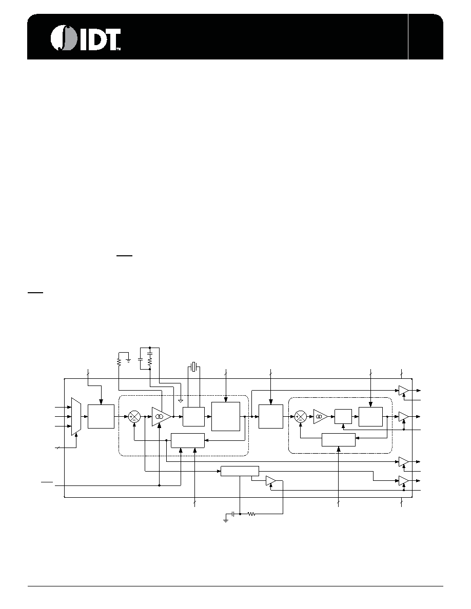
Block Diagram
C harge
Pum p
VC XO
P u lla b le
xtal
VC LK
X2
X1
ISET
4
VD D
4
CL R
LF
FV D iv ide r
1-4096
RV
Div id e r
1 ,2,4,1 2 8
SV
Div id e r
1,2 ,4,6,8,
10,12,16
IC L K 2
IC L K 1
MX 1 :0
0X
RV 1 :0
2
RT
Div id e r
1-4
Ph ase
De te cto r
VC XO
PLL
FT D iv ide r
1-64
ST
Div id e r
2,4 ,8,1 6
VC O
T ran slato r
PL L
SV 2 :0
3
F V 11:0
FT5 :0
6
ST1 :0
2
TC LK
OE V
OE T
IC L K 0
10
01
2
LD
OE L
GN D
RCL K
OE R
Lo c k D e tector
12
LD C
LD R
LF R
RT 1 :0
2
相关PDF资料 |
PDF描述 |
|---|---|
| MK2069-01GITR | 160 MHz, OTHER CLOCK GENERATOR, PDSO56 |
| MK2069-01GI | 160 MHz, OTHER CLOCK GENERATOR, PDSO56 |
| MK2069-02GILF | 160 MHz, OTHER CLOCK GENERATOR, PDSO56 |
| MK2069-02GITR | 160 MHz, OTHER CLOCK GENERATOR, PDSO56 |
| MK2069-02GILFTR | 160 MHz, OTHER CLOCK GENERATOR, PDSO56 |
相关代理商/技术参数 |
参数描述 |
|---|---|
| MK2069-01GITR | 功能描述:IC VCXO CLK SYNCHRONIZER 56TSSOP RoHS:否 类别:集成电路 (IC) >> 时钟/计时 - 时钟发生器,PLL,频率合成器 系列:- 标准包装:39 系列:- 类型:* PLL:带旁路 输入:时钟 输出:时钟 电路数:1 比率 - 输入:输出:1:10 差分 - 输入:输出:是/是 频率 - 最大:170MHz 除法器/乘法器:无/无 电源电压:2.375 V ~ 3.465 V 工作温度:0°C ~ 70°C 安装类型:* 封装/外壳:* 供应商设备封装:* 包装:* |
| MK2069-03 | 制造商:ICS 制造商全称:ICS 功能描述:VCXO-Based Clock Translator with High Multiplication |
| MK2069-03GI | 功能描述:IC VCXO CLK TRANSLATOR 56-TSSOP RoHS:否 类别:集成电路 (IC) >> 时钟/计时 - 时钟发生器,PLL,频率合成器 系列:- 标准包装:27 系列:Precision Edge® 类型:频率合成器 PLL:是 输入:PECL,晶体 输出:PECL 电路数:1 比率 - 输入:输出:1:1 差分 - 输入:输出:无/是 频率 - 最大:800MHz 除法器/乘法器:是/无 电源电压:3.135 V ~ 5.25 V 工作温度:0°C ~ 85°C 安装类型:表面贴装 封装/外壳:28-SOIC(0.295",7.50mm 宽) 供应商设备封装:28-SOIC 包装:管件 |
| MK2069-03GITR | 功能描述:时钟发生器及支持产品 VCXO-BASED CLOCK TRANSLATOR RoHS:否 制造商:Silicon Labs 类型:Clock Generators 最大输入频率:14.318 MHz 最大输出频率:166 MHz 输出端数量:16 占空比 - 最大:55 % 工作电源电压:3.3 V 工作电源电流:1 mA 最大工作温度:+ 85 C 安装风格:SMD/SMT 封装 / 箱体:QFN-56 |
| MK2069-04 | 制造商:ICS 制造商全称:ICS 功能描述:VCXO-Based Universal Clock Translator |
发布紧急采购,3分钟左右您将得到回复。