- 您现在的位置:买卖IC网 > PDF目录45328 > MK2069-01GILFTR (INTEGRATED DEVICE TECHNOLOGY INC) 160 MHz, OTHER CLOCK GENERATOR, PDSO56 PDF资料下载
参数资料
| 型号: | MK2069-01GILFTR |
| 厂商: | INTEGRATED DEVICE TECHNOLOGY INC |
| 元件分类: | 时钟产生/分配 |
| 英文描述: | 160 MHz, OTHER CLOCK GENERATOR, PDSO56 |
| 封装: | 6.10 MM, 0.50 MM PITCH, TSSOP-56 |
| 文件页数: | 3/21页 |
| 文件大小: | 211K |
| 代理商: | MK2069-01GILFTR |
MK2069-01
VCXO-BASED LINE CARD CLOCK SYNCHRONIZER
VCXO AND SYNTHESIZER
IDT VCXO-BASED LINE CARD CLOCK SYNCHRONIZER
11
MK2069-01
REV K 051310
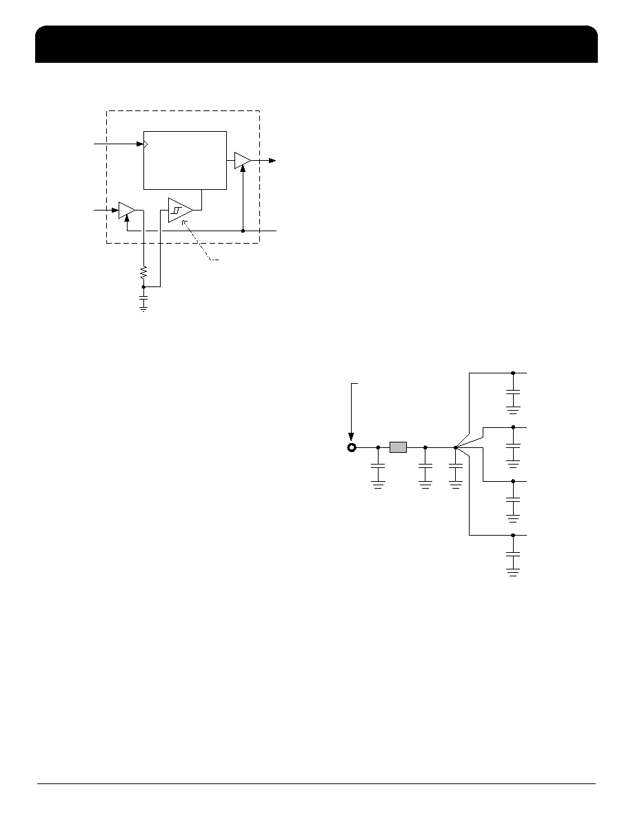
Lock Detection Circuit Diagram
If the lock detection circuit is not used, the LDR output may
remain unconnected, however the LDC input should be tied
high or low. If the PCB was designed to accommodate the
RLD and CLD components but the LD output will not be
used, RLD can remain unstuffed and CLD can be replaced
with a resistor (< 10 kohm).
Power Supply Considerations
As with any integrated clock device, the MK2069-01 has a
special set of power supply requirements:
The feed from the system power supply must be filtered
for noise that can cause output clock jitter. Power supply
noise sources include the system switching power supply
or other system components. The noise can interfere with
device PLL components such as the VCO or phase
detector.
Each VDD pin must be decoupled individually to prevent
power supply noise generated by one device circuit block
from interfering with another circuit block.
Clock noise from device VDD pins must not get onto the
PCB power plane or system EMI problems may result.
This above set of requirements is served by the circuit
illustrated in the Recommended Power Supply Connection
(next page). The main features of this circuit are as follows:
Only one connection is made to the PCB power plane.
The capacitors and ferrite chip (or ferrite bead) on the
common device supply form a lowpass ‘pi’ filter that
remove noise from the power supply as well as clock
noise back toward the supply. The bulk capacitor should
be a tantalum type, 1
μF minimum. The other capacitors
should be ceramic type.
The power supply traces to the individual VDD pins
should fan out at the common supply filter to reduce
interaction between the device circuit blocks.
The decoupling capacitors at the VDD pins should be
ceramic type and should be as close to the VDD pin as
possible. There should be no via’s between the
decoupling capacitor and the supply pin.
Recommended Power Supply Connection
Series Termination Resistor
Output clock PCB traces over 1 inch should use series
termination to maintain clock signal integrity and to reduce
EMI. To series terminate a 50
Ω trace, which is a commonly
used PCB trace impedance, place a 33
Ω resistor in series
with the clock line as close to the clock output pin as
possible. The nominal impedance of the clock output is 20
Ω.
Lo c k D e te c tio n C irc uit
Lo c k
Q u a lific a tio n
C ounte r
(8 up , 1 dow n)
VC XO
Ph a s e
De te c to r
Erro r
Ou tp u t
LD
LD C
LD R
RL D
CL D
R ESET
FV
Div id e r
Ou tp u t
OE L
Input Th re s hold
s e t to V D D /2
Connection Via to 3.3V
Power Plane
Ferrite
Chip
0.
1
F
BU
L
K
1
nF
VDD
Pin
0.
01
F
VDD
Pin
0.
0
1
F
VDD
Pin
0.
01
F
VDD
Pin
0.
01
F
相关PDF资料 |
PDF描述 |
|---|---|
| MK2069-01GITR | 160 MHz, OTHER CLOCK GENERATOR, PDSO56 |
| MK2069-01GI | 160 MHz, OTHER CLOCK GENERATOR, PDSO56 |
| MK2069-02GILF | 160 MHz, OTHER CLOCK GENERATOR, PDSO56 |
| MK2069-02GITR | 160 MHz, OTHER CLOCK GENERATOR, PDSO56 |
| MK2069-02GILFTR | 160 MHz, OTHER CLOCK GENERATOR, PDSO56 |
相关代理商/技术参数 |
参数描述 |
|---|---|
| MK2069-01GITR | 功能描述:IC VCXO CLK SYNCHRONIZER 56TSSOP RoHS:否 类别:集成电路 (IC) >> 时钟/计时 - 时钟发生器,PLL,频率合成器 系列:- 标准包装:39 系列:- 类型:* PLL:带旁路 输入:时钟 输出:时钟 电路数:1 比率 - 输入:输出:1:10 差分 - 输入:输出:是/是 频率 - 最大:170MHz 除法器/乘法器:无/无 电源电压:2.375 V ~ 3.465 V 工作温度:0°C ~ 70°C 安装类型:* 封装/外壳:* 供应商设备封装:* 包装:* |
| MK2069-03 | 制造商:ICS 制造商全称:ICS 功能描述:VCXO-Based Clock Translator with High Multiplication |
| MK2069-03GI | 功能描述:IC VCXO CLK TRANSLATOR 56-TSSOP RoHS:否 类别:集成电路 (IC) >> 时钟/计时 - 时钟发生器,PLL,频率合成器 系列:- 标准包装:27 系列:Precision Edge® 类型:频率合成器 PLL:是 输入:PECL,晶体 输出:PECL 电路数:1 比率 - 输入:输出:1:1 差分 - 输入:输出:无/是 频率 - 最大:800MHz 除法器/乘法器:是/无 电源电压:3.135 V ~ 5.25 V 工作温度:0°C ~ 85°C 安装类型:表面贴装 封装/外壳:28-SOIC(0.295",7.50mm 宽) 供应商设备封装:28-SOIC 包装:管件 |
| MK2069-03GITR | 功能描述:时钟发生器及支持产品 VCXO-BASED CLOCK TRANSLATOR RoHS:否 制造商:Silicon Labs 类型:Clock Generators 最大输入频率:14.318 MHz 最大输出频率:166 MHz 输出端数量:16 占空比 - 最大:55 % 工作电源电压:3.3 V 工作电源电流:1 mA 最大工作温度:+ 85 C 安装风格:SMD/SMT 封装 / 箱体:QFN-56 |
| MK2069-04 | 制造商:ICS 制造商全称:ICS 功能描述:VCXO-Based Universal Clock Translator |
发布紧急采购,3分钟左右您将得到回复。