- 您现在的位置:买卖IC网 > PDF目录65811 > MK2771-05S 50 MHz, OTHER CLOCK GENERATOR, PDSO20 PDF资料下载
参数资料
| 型号: | MK2771-05S |
| 元件分类: | 时钟产生/分配 |
| 英文描述: | 50 MHz, OTHER CLOCK GENERATOR, PDSO20 |
| 封装: | SOIC-20 |
| 文件页数: | 3/4页 |
| 文件大小: | 103K |
| 代理商: | MK2771-05S |
MK2771-05
VCXO and Set-Top Clock Source
MDS2771-05B
3
Revision 2038
Printed 11/8/99
MicroClock Division of ICS1271 Parkmoor Ave.San JoseCA95126(408)295-9800tel(408)295-9818fax
ICRO
CLOCK
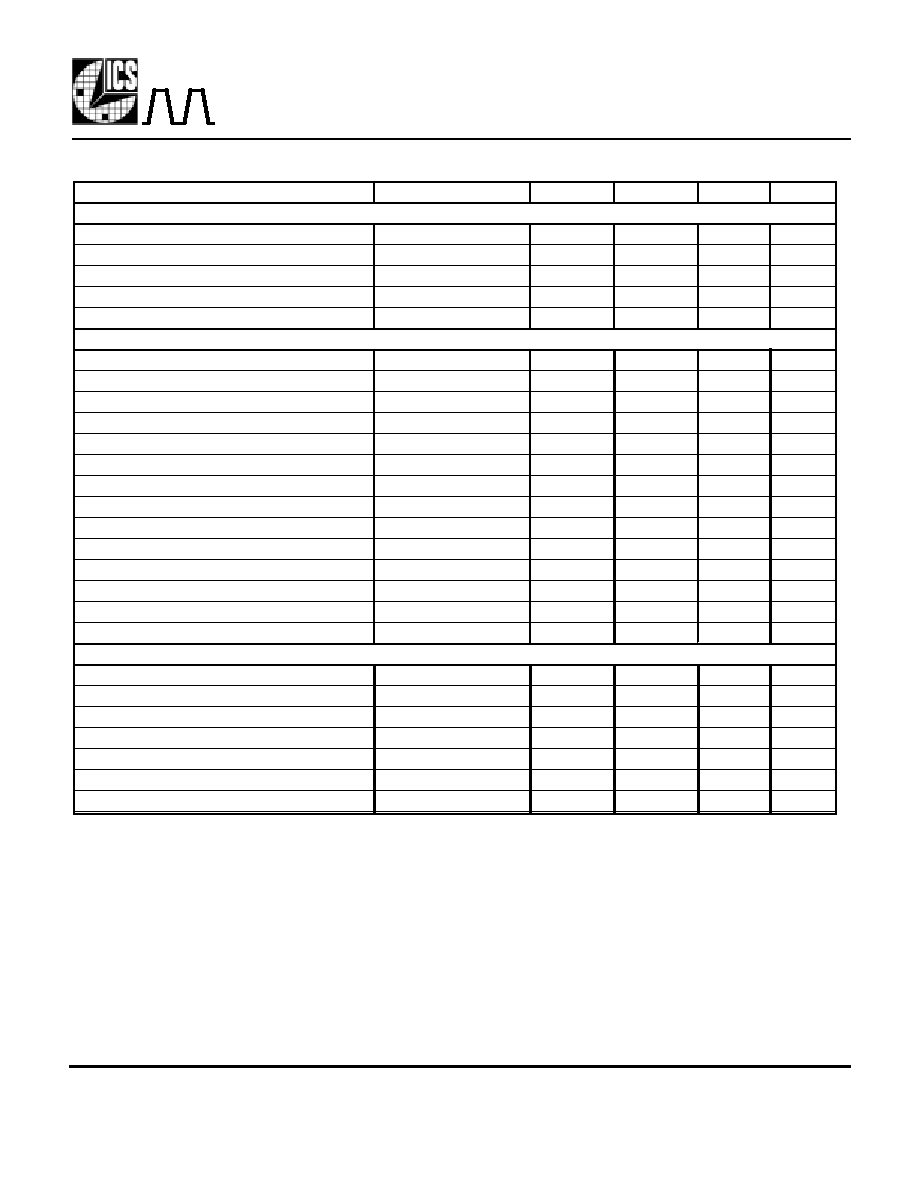
Parameter
Conditions
Minimum
Typical
Maximum
Units
ABSOLUTE MAXIMUM RATINGS (n
note 1)
Supply voltage, VDD
Referenced to GND
7
V
Inputs and Clock Outputs
Referenced to GND
-0.5
VDD+0.5
V
Ambient Operating Temperature
0
70
°C
Soldering Temperature
Max of 10 seconds
260
°C
Storage temperature
-65
150
°C
DC CHARACTERISTICS (VDD = 5.0V
V unless noted)
Operating Voltage, VDD
4.75
5.25
V
Input High Voltage, VIH, X1 pin only
3.5
2.5
V
Input Low Voltage, VIL, X1 pin only
2.5
1.5
V
Input High Voltage, VIH (ACS,PCS1)
VDD-0.5
V
Input High Voltage, VIH (PCS0)
2
V
Input Low Voltage, VIL
0.8
V
Output High Voltage, VOH
IOH=-25mA
2.4
V
Output Low Voltage, VOL
IOL=25mA
0.4
V
Output High Voltage, VOH, CMOS level
IOH=-8mA
VDD-0.4
V
Operating Supply Current, IDD
No Load, note 2
60
mA
Short Circuit Current
Each output
±100
mA
Input Capacitance
7
pF
Frequency synthesis error
All clocks as shown
0
1
ppm
VIN, VCXO control voltage
0
3
V
AC CHARACTERISTICS (VDD = 5.0V
V unless noted)
Input Crystal Frequency
14.31818
MHz
Input Crystal Accuracy
±30
ppm
Output Clock Rise Time
0.8 to 2.0V
1.5
ns
Output Clock Fall Time
2.0 to 0.8V
1.5
ns
Output Clock Duty Cycle
At 1.4V
40
60
%
Maximum Absolute Jitter, short term
300
ps
27 MHz output pullability, note 3
0V
VIN
3V
±100
ppm
Electrical Specifications
Notes:
1. Stresses beyond those listed under Absolute Maximum Ratings could cause permanent damage to the device. Prolonged
exposure to levels above the operating limits but below the Absolute Maximums may affect device reliability.
2. With ACLK at 22.5792 MHz and PCLK at 50 MHz.
3. With a
±150ppm pullable cr stal.
External Components/Cr stal Selection
The MK2771-05 requires a minimum number of external components for proper operation. Decoupling capacitors of 0.1
F
should be connected between VDD (pin 15) and GND (14), and betweeen AVDD (4) and GND (7), as close to the MK2771-05 as
possible. A series termination resistor of 33
may be used for each clock output. The input crystal must be connected as close to the
chip as possible. The 14.31818 MHz input crystal should be a parallel mode, pullable, AT cut with 16.0pF load capacitance. Consult
MicroClock for recommended suppliers. Only the crystal should be connected to X1 and X2 - do not connect external load
capacitors to the crystal pins. Do not connect the crystal case (can) to ground, and do not place a ground plane underneath the crytal
traces connected to pins 2 and 3. Refer to MicroClock Application Note MAN05 for additional information.
≤
相关PDF资料 |
PDF描述 |
|---|---|
| MK2771-05STR | 50 MHz, OTHER CLOCK GENERATOR, PDSO20 |
| MK2771-16RTR | 50 MHz, OTHER CLOCK GENERATOR, PDSO28 |
| MK2771-16R | 50 MHz, OTHER CLOCK GENERATOR, PDSO28 |
| MK2771-16RLF | 50 MHz, OTHER CLOCK GENERATOR, PDSO28 |
| MK3200SLF | 0.032768 MHz, OTHER CLOCK GENERATOR, PDSO8 |
相关代理商/技术参数 |
参数描述 |
|---|---|
| MK2771-12 | 制造商:ICS 制造商全称:ICS 功能描述:VCXO and Set-Top Clock Source |
| MK2771-12S | 制造商:ICS 制造商全称:ICS 功能描述:VCXO and Set-Top Clock Source |
| MK2771-12STR | 制造商:ICS 制造商全称:ICS 功能描述:VCXO and Set-Top Clock Source |
| MK2771-13 | 制造商:ICS 制造商全称:ICS 功能描述:VCXO and Set-Top Clock Source |
| MK2771-13S | 制造商:ICS 制造商全称:ICS 功能描述:VCXO and Set-Top Clock Source |
发布紧急采购,3分钟左右您将得到回复。