- 您现在的位置:买卖IC网 > PDF目录22222 > ML4824CP1 (Fairchild Semiconductor)IC PFC CTRLR AVERAGE CURR 16DIP PDF资料下载
参数资料
| 型号: | ML4824CP1 |
| 厂商: | Fairchild Semiconductor |
| 文件页数: | 10/15页 |
| 文件大小: | 103K |
| 描述: | IC PFC CTRLR AVERAGE CURR 16DIP |
| 标准包装: | 25 |
| 模式: | 平均电流 |
| 频率 - 开关: | 76kHz |
| 电流 - 启动: | 700µA |
| 电源电压: | 10.5 V ~ 13.2 V |
| 工作温度: | 0°C ~ 70°C |
| 安装类型: | 通孔 |
| 封装/外壳: | 16-DIP(0.300",7.62mm) |
| 供应商设备封装: | 16-DIP |
| 包装: | 管件 |
| 产品目录页面: | 1222 (CN2011-ZH PDF) |
| 其它名称: | ML4824CP1_NL ML4824CP1_NL-ND |
ML4824
PRODUCT SPECIFICATION
10
REV. 1.0.6 11/7/03
V
IN
OK Comparator
The V
IN
OK comparator monitors the DC output of the PFC
and inhibits the PWM if this voltage on V
FB
is less than
its nominal 2.5V. Once this voltage reaches 2.5V, which
corresponds to the PFC output capacitor being charged to its
rated boost voltage, the soft-start begins.
PWM Control (RAMP 2)
When the PWM section is used in current mode, RAMP 2 is
generally used as the sampling point for a voltage represent-
ing the current in the primary of the PWMs output trans-
former, derived either by a current sensing resistor or a
current transformer. In voltage mode, it is the input for a
ramp voltage generated by a second set of timing compo-
nents (R
RAMP2
, C
RAMP2
), which will have a minimum
value of zero volts and should have a peak value of approxi-
mately 5V. In voltage mode operation, feedforward from the
PFC output buss is an excellent way to derive the timing
ramp for the PWM stage.
Soft Start
Start-up of the PWM is controlled by the selection of the
external capacitor at SS. A current source of 50礎 supplies
the charging current for the capacitor, and start-up of the
PWM begins at 1.25V. Start-up delay can be programmed by
the following equation::
where C
SS
is the required soft start capacitance, and t
DELAY
is the desired start-up delay.
It is important that the time constant of the PWM soft-start
allow the PFC time to generate sufcient output power for
the PWM section. The PWM start-up delay should be at least
5ms.
Solving for the minimum value of C
SS
:
Caution should be exercised when using this minimum soft
start capacitance value because premature charging of the SS
capacitor and activation of the PWM section can result if
V
FB
is in the hysteresis band of the V
IN
OK comparator at
start-up. The magnitude of V
FB
at start-up is related both to
line voltage and nominal PFC output voltage. Typically, a
1.0礔 soft start capacitor will allow time for V
FB
and PFC
out to reach their nominal values prior to activation of the
PWM section at line voltages between 90Vrms and
265Vrms.
GENERATING V
CC
The ML4824 is a current-fed part. It has an internal shunt
voltage regulator, which is designed to regulate the voltage
internal to the part at 13.5V. This allows a low power dissipa-
tion while at the same time delivering 10V of gate drive at
the PWM OUT and PFC OUT outputs. It is important to
limit the current through the part to avoid overheating or
destroying it. This can be easily done with a single resistor in
series with the Vcc pin, returned to a bias supply of typically
18V to 20V. The resistors value must be chosen to meet the
operating current requirement of the ML4824 itself (19mA
max) plus the current required by the two gate driver outputs.
EXAMPLE:
With a VBIAS of 20V, a VCC limit of 14.6V (max) and the
ML4824 driving a total gate charge of 110nC at 100kHz
(e.g., 1 IRF840 MOSFET and 2 IRF830 MOSFETs), the
gate driver current required is:
To check the maximum dissipation in the ML4824, nd the
current at the minimum V
CC
(12.4V)::
The maximum allowable I
CC
is 55mA, so this is an accept-
able design.
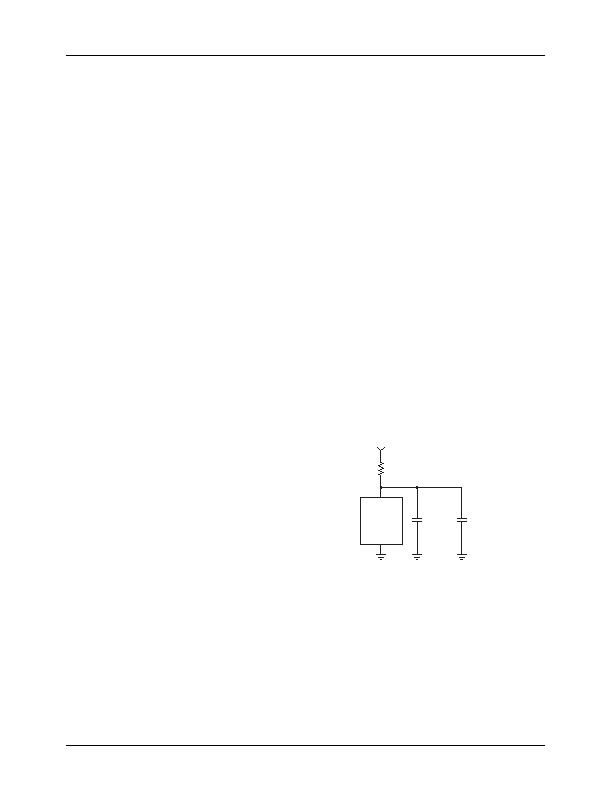
The ML4824 should be locally bypassed with a 10nF and a
1礔 ceramic capacitor. In most applications, an electrolytic
capacitor of between 100礔 and 330礔 is also required
across the part, both for ltering and as part of the start-up
bootstrap circuitry.
Figure 3. External Component Connections to V
CC
Leading/Trailing Modulation
Conventional Pulse Width Modulation (PWM) techniques
employ trailing edge modulation in which the switch will
turn on right after the trailing edge of the system clock.
The error amplier output voltage is then compared with the
modulating ramp. When the modulating ramp reaches the
level of the error amplier output voltage, the switch will be
turned OFF. When the switch is ON, the inductor current will
ramp up. The effective duty cycle of the trailing edge modu-
lation is determined during the ON time of the switch. Figure
4 shows a typical trailing edge control scheme.
C
SS
t
DELAY
50礎
1.25V
--------------- -
?/DIV>
=
(6)
C
SS
5ms
50礎
1.25V
--------------- -
?/DIV>
200nF
=
=
I
GATEDRIVE
100kHz 100nC
?/DIV>
11mA
=
=
(7)
R
BIAS
20V 14.6V
19mA 11mA
+
-------------------------------------- -
180&
=
=
(8)
I
CC
20V 12.4V
180&
-------------------------------- -
42.2mA
=
=
(9)
ML4824
V
CC
GND
V
BIAS
10nF
CERAMIC
1礔
CERAMIC
R
BIAS
相关PDF资料 |
PDF描述 |
|---|---|
| VI-J7T-IZ | CONVERTER MOD DC/DC 6.5V 25W |
| 195D476X0016R2T | CAP TANT 47UF 16V 20% 2824 |
| HBC49DREN-S13 | CONN EDGECARD 98POS .100 EXTEND |
| VI-J7R-IZ | CONVERTER MOD DC/DC 7.5V 25W |
| SRR1280-821K | INDUCTOR POWER 820UH 0.70A SMD |
相关代理商/技术参数 |
参数描述 |
|---|---|
| ML4824CP-1 | 制造商:MICRO-LINEAR 制造商全称:MICRO-LINEAR 功能描述:Power Factor Correction and PWM Controller Combo |
| ML4824CP1"32 | 制造商:Fairchild Semiconductor Corporation 功能描述:Power Factor Controller IC |
| ML4824CP1_Q | 功能描述:功率因数校正 IC PFC Controller PWM Combo RoHS:否 制造商:Fairchild Semiconductor 开关频率:300 KHz 最大功率耗散: 最大工作温度:+ 125 C 安装风格:SMD/SMT 封装 / 箱体:SOIC-8 封装:Reel |
| ML4824CP2 | 功能描述:功率因数校正 IC PFC Controller PWM Combo RoHS:否 制造商:Fairchild Semiconductor 开关频率:300 KHz 最大功率耗散: 最大工作温度:+ 125 C 安装风格:SMD/SMT 封装 / 箱体:SOIC-8 封装:Reel |
| ML4824CP-2 | 制造商:MICRO-LINEAR 制造商全称:MICRO-LINEAR 功能描述:Power Factor Correction and PWM Controller Combo |
发布紧急采购,3分钟左右您将得到回复。