- 您现在的位置:买卖IC网 > PDF目录22222 > ML4824CP1 (Fairchild Semiconductor)IC PFC CTRLR AVERAGE CURR 16DIP PDF资料下载
参数资料
| 型号: | ML4824CP1 |
| 厂商: | Fairchild Semiconductor |
| 文件页数: | 8/15页 |
| 文件大小: | 103K |
| 描述: | IC PFC CTRLR AVERAGE CURR 16DIP |
| 标准包装: | 25 |
| 模式: | 平均电流 |
| 频率 - 开关: | 76kHz |
| 电流 - 启动: | 700µA |
| 电源电压: | 10.5 V ~ 13.2 V |
| 工作温度: | 0°C ~ 70°C |
| 安装类型: | 通孔 |
| 封装/外壳: | 16-DIP(0.300",7.62mm) |
| 供应商设备封装: | 16-DIP |
| 包装: | 管件 |
| 产品目录页面: | 1222 (CN2011-ZH PDF) |
| 其它名称: | ML4824CP1_NL ML4824CP1_NL-ND |
ML4824
PRODUCT SPECIFICATION
8
REV. 1.0.6 11/7/03
3. The output of the voltage error amplier, VEAO. The
gain modulator responds linearly to variations in this
voltage.
The output of the gain modulator is a current signal, in the
form of a full wave rectied sinusoid at twice the line
frequency. This current is applied to the virtual-ground
(negative) input of the current error amplier. In this way
the gain modulator forms the reference for the current error
loop, and ultimately controls the instantaneous current draw
of the PFC from the power line. The general form for the
output of the gain modulator is:
More exactly, the output current of the gain modulator is
given by:
where K is in units of V
-1
.
Note that the output current of the gain modulator is limited
to E 200礎.
Current Error Amplier
The current error ampliers output controls the PFC duty
cycle to keep the average current through the boost inductor
a linear function of the line voltage. At the inverting input to
the current error amplier, the output current of the gain
modulator is summed with a current which results from a
negative voltage being impressed upon the I
SENSE
pin
(current into I
SENSE
E V
SENSE
/3.5k&). The negative
voltage on I
SENSE
represents the sum of all currents owing
in the PFC circuit, and is typically derived from a current
sense resistor in series with the negative terminal of the input
bridge rectier. In higher power applications, two current
transformers are sometimes used, one to monitor the I
D
of
the boost MOSFET(s) and one to monitor the I
F
of the boost
diode. As stated above, the inverting input of the current
error amplier is a virtual ground. Given this fact, and the
arrangement of the duty cycle modulator polarities internal
to the PFC, an increase in positive current from the gain
modulator will cause the output stage to increase its duty
cycle until the voltage on I
SENSE
is adequately negative to
cancel this increased current. Similarly, if the gain modula-
tors output decreases, the output duty cycle will decrease, to
achieve a less negative voltage on the I
SENSE
pin.
Cycle-By-Cycle Current Limiter
The ISENSE pin, as well as being a part of the current
feedback loop, is a direct input to the cycle-by-cycle current
limiter for the PFC section. Should the input voltage at this
pin ever be more negative than -1V, the output of the PFC
will be disabled until the protection ip-op is reset by the
clock pulse at the start of the next PFC power cycle.
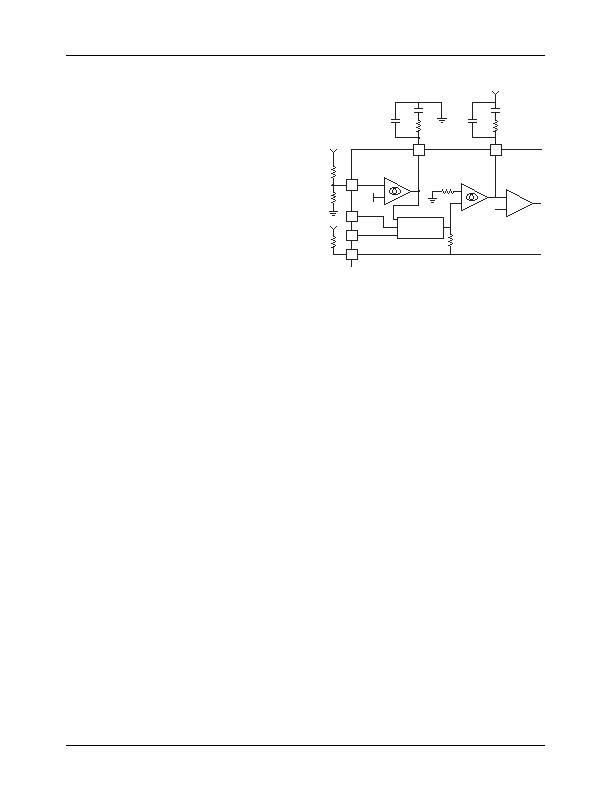
Figure 2. Compensation Network Connections for the
Voltage and Current Error Amplifiers
Overvoltage Protection
The OVP comparator serves to protect the power circuit
from being subjected to excessive voltages if the load should
suddenly change. A resistor divider from the high voltage
DC output of the PFC is fed to V
FB
. When the voltage on
V
FB
exceeds 2.7V, the PFC output driver is shut down. The
PWM section will continue to operate. The OVP comparator
has 125mV of hysteresis, and the PFC will not restart until
the voltage at V
FB
drops below 2.58V. The V
FB
should be
set at a level where the active and passive external power
components and the ML4824 are within their safe operating
voltages, but not so low as to interfere with the boost voltage
regulation loop.
Error Amplier Compensation
The PWM loading of the PFC can be modeled as a negative
resistor; an increase in input voltage to the PWM causes a
decrease in the input current. This response dictates the
proper compensation of the two transconductance error
ampliers. Figure 2 shows the types of compensation
networks most commonly used for the voltage and current
error ampliers, along with their respective return points.
The current loop compensation is returned to V
REF
to
produce a soft-start characteristic on the PFC: as the
reference voltage comes up from zero volts, it creates a
differentiated voltage on IEAO which prevents the PFC
from immediately demanding a full duty cycle on its boost
converter.
There are two major concerns when compensating the
voltage loop error amplier; stability and transient response.
Optimizing interaction between transient response and
stability requires that the error ampliers open-loop
crossover frequency should be 1/2 that of the line frequency,
or 23Hz for a 47Hz line (lowest anticipated international
power frequency). The gain vs. input voltage of the
I
GAINMOD
I
AC
VEAO
?/DIV>
V
RMS
2
------------------------------- - 1V
?/DIV>
E
(1)
I
GAINMOD
K VEAO 1.5V
(
)
?/DIV>
I
AC
?/DIV>
E
15
VEAO
IEAO
V
FB
I
AC
V
RMS
I
SENSE
2.5V
+
16
2
4
3
VEA
+
IEA
+
V
REF
1
PFC
OUTPUT
GAIN
MODULATOR
相关PDF资料 |
PDF描述 |
|---|---|
| VI-J7T-IZ | CONVERTER MOD DC/DC 6.5V 25W |
| 195D476X0016R2T | CAP TANT 47UF 16V 20% 2824 |
| HBC49DREN-S13 | CONN EDGECARD 98POS .100 EXTEND |
| VI-J7R-IZ | CONVERTER MOD DC/DC 7.5V 25W |
| SRR1280-821K | INDUCTOR POWER 820UH 0.70A SMD |
相关代理商/技术参数 |
参数描述 |
|---|---|
| ML4824CP-1 | 制造商:MICRO-LINEAR 制造商全称:MICRO-LINEAR 功能描述:Power Factor Correction and PWM Controller Combo |
| ML4824CP1"32 | 制造商:Fairchild Semiconductor Corporation 功能描述:Power Factor Controller IC |
| ML4824CP1_Q | 功能描述:功率因数校正 IC PFC Controller PWM Combo RoHS:否 制造商:Fairchild Semiconductor 开关频率:300 KHz 最大功率耗散: 最大工作温度:+ 125 C 安装风格:SMD/SMT 封装 / 箱体:SOIC-8 封装:Reel |
| ML4824CP2 | 功能描述:功率因数校正 IC PFC Controller PWM Combo RoHS:否 制造商:Fairchild Semiconductor 开关频率:300 KHz 最大功率耗散: 最大工作温度:+ 125 C 安装风格:SMD/SMT 封装 / 箱体:SOIC-8 封装:Reel |
| ML4824CP-2 | 制造商:MICRO-LINEAR 制造商全称:MICRO-LINEAR 功能描述:Power Factor Correction and PWM Controller Combo |
发布紧急采购,3分钟左右您将得到回复。