- 您现在的位置:买卖IC网 > PDF目录45333 > ML9040A-AXXWA (OKI ELECTRIC INDUSTRY CO LTD) 16 X 40 DOTS DOT MAT LCD DRVR AND DSPL CTLR, UUC81 PDF资料下载
参数资料
| 型号: | ML9040A-AXXWA |
| 厂商: | OKI ELECTRIC INDUSTRY CO LTD |
| 元件分类: | 显示控制器 |
| 英文描述: | 16 X 40 DOTS DOT MAT LCD DRVR AND DSPL CTLR, UUC81 |
| 封装: | ALUMINUM PAD, DIE-81 |
| 文件页数: | 5/49页 |
| 文件大小: | 515K |
| 代理商: | ML9040A-AXXWA |
第1页第2页第3页第4页当前第5页第6页第7页第8页第9页第10页第11页第12页第13页第14页第15页第16页第17页第18页第19页第20页第21页第22页第23页第24页第25页第26页第27页第28页第29页第30页第31页第32页第33页第34页第35页第36页第37页第38页第39页第40页第41页第42页第43页第44页第45页第46页第47页第48页第49页
ML9040A-Axx/-Bxx
Semiconductor
13/49
PEDL9040A-03
FUNCTIONAL DESCRIPTION
Instruction Register (IR) and Data Register (DR)
These two registers are selected by the REGISTER SELECTION (RS) pin.
The DR is selected when the "H" level is input to the RS pin and IR is selected when the "L"
level is input.
The IR is used to store the address of the display data RAM (DD RAM) or character
generator RAM (CG RAM) and instruction code.
The IR can be written, but not be read by the microcomputer (CPU).
The DR is used to write and read the data to and from the DD RAM or CG RAM.
The data written to DR by the CPU is automatically written to the DD RAM or CG RAM
as an internal operation.
When an address code is written to IR, the data (of the specified address) is automatically
transferred from the DD RAM or CG RAM to the DR. Next, when the CPU reads the DR,
it is possible to verify DD RAM or CG RAM data from the DR data.
After the writing of DR by the CPU, the next adress in the DD RAM or CG RAM is selected
to be ready for the next CPU writing.
Likewise, after the reading out of DR by the CPU, DD RAM or CG RAM data is read out
by the DR to be ready for the next CPU reading.
Write/read to and from both registers is carried out by the READ/WRITE (R/W) pin.
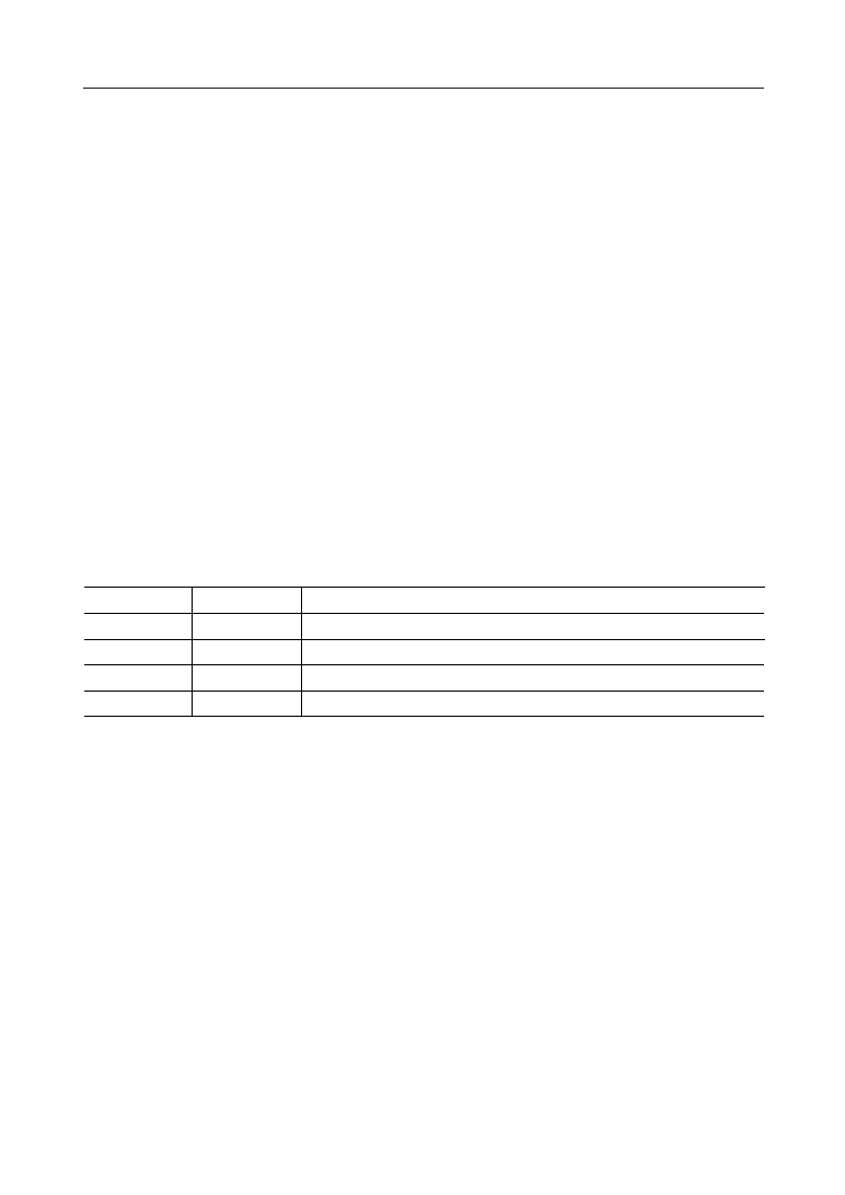
Table 1 RS and R/W pins functions
Busy Flag (BF)
When the busy flag is at "H", it indicates that the ML9040A-Axx/-Bxx is engaged in internal
operation.
When the busy flag is at "H", any new instruction is ignored.
When R/W = "H" and RS = "L", the busy flag is output from DB7.
New instruction should be input when busy flag is "L" level.
When the busy flag is at "H", the output code of the address counter (ADC) is undefined.
Address Counter (ADC)
The address counter (ADC) allocates the address for the DD RAM and CG RAM write/
read and also for the cursor display.
When the instruction code for a DD RAM address or CG RAM address setting is input to
IR, after deciding whether it is DD RAM or CG RAM, the address code is transferred from
IR to ADC. After writing (reading) the display data to (from) the DD RAM or CG RAM,
the ADC is incremented (decremented) by 1 internally.
The data of the ADC is output to DB0 - DB6 on the conditions that R/W = "H", RS = "L", and
BF = "L".
L
RS
Function
R/W
L
IR write
H
L
Read of busy flag (BF) and address counter (ADC)
L
H
DR write
H
DR read
相关PDF资料 |
PDF描述 |
|---|---|
| ML9040A-BXXGA | 16 X 40 DOTS DOT MAT LCD DRVR AND DSPL CTLR, PQFP80 |
| ML9040A-AXXWA | 16 X 40 DOTS DOT MAT LCD DRVR AND DSPL CTLR, UUC81 |
| ML9040A-BXXWA | 16 X 40 DOTS DOT MAT LCD DRVR AND DSPL CTLR, UUC81 |
| ML9041A-01ACVWA | 17 X 100 DOTS DOT MAT LCD DRVR AND DSPL CTLR, UUC189 |
| ML9041A-01ACVWA | 17 X 100 DOTS DOT MAT LCD DRVR AND DSPL CTLR, UUC189 |
相关代理商/技术参数 |
参数描述 |
|---|---|
| ML9040A-B01GAZ03A-7 | 功能描述:LCD 驱动器 LCD DOT Matrix Controller, 16/40 RoHS:否 制造商:Maxim Integrated 数位数量:4.5 片段数量:30 最大时钟频率:19 KHz 工作电源电压:3 V to 3.6 V 最大工作温度:+ 85 C 最小工作温度:- 20 C 封装 / 箱体:PDIP-40 封装:Tube |
| ML9040A-BXX | 制造商:OKI 制造商全称:OKI electronic componets 功能描述:DOT MATRIX LCD CONTROLLER WITH 16-DOT COMMON DRIVER AND 40-DOT SEGMENT DRIVER |
| ML9040A-BXXGA | 制造商:OKI 制造商全称:OKI electronic componets 功能描述:DOT MATRIX LCD CONTROLLER WITH 16-DOT COMMON DRIVER AND 40-DOT SEGMENT DRIVER |
| ML9040A-BXXWA | 制造商:OKI 制造商全称:OKI electronic componets 功能描述:DOT MATRIX LCD CONTROLLER WITH 16-DOT COMMON DRIVER AND 40-DOT SEGMENT DRIVER |
| ML9040-AXX | 制造商:OKI 制造商全称:OKI electronic componets 功能描述:DOT MATRIX LCD CONTROLLER WITH 16-DOT COMMON DRIVER AND 40-DOT SEGMENT DRIVER |
发布紧急采购,3分钟左右您将得到回复。