- 您现在的位置:买卖IC网 > PDF目录182950 > MM74HC4040J (FAIRCHILD SEMICONDUCTOR CORP) HC/UH SERIES, ASYN NEGATIVE EDGE TRIGGERED 12-BIT UP BINARY COUNTER, CDIP16 PDF资料下载
参数资料
| 型号: | MM74HC4040J |
| 厂商: | FAIRCHILD SEMICONDUCTOR CORP |
| 元件分类: | 计数器 |
| 英文描述: | HC/UH SERIES, ASYN NEGATIVE EDGE TRIGGERED 12-BIT UP BINARY COUNTER, CDIP16 |
| 封装: | DIP-16 |
| 文件页数: | 2/8页 |
| 文件大小: | 189K |
| 代理商: | MM74HC4040J |
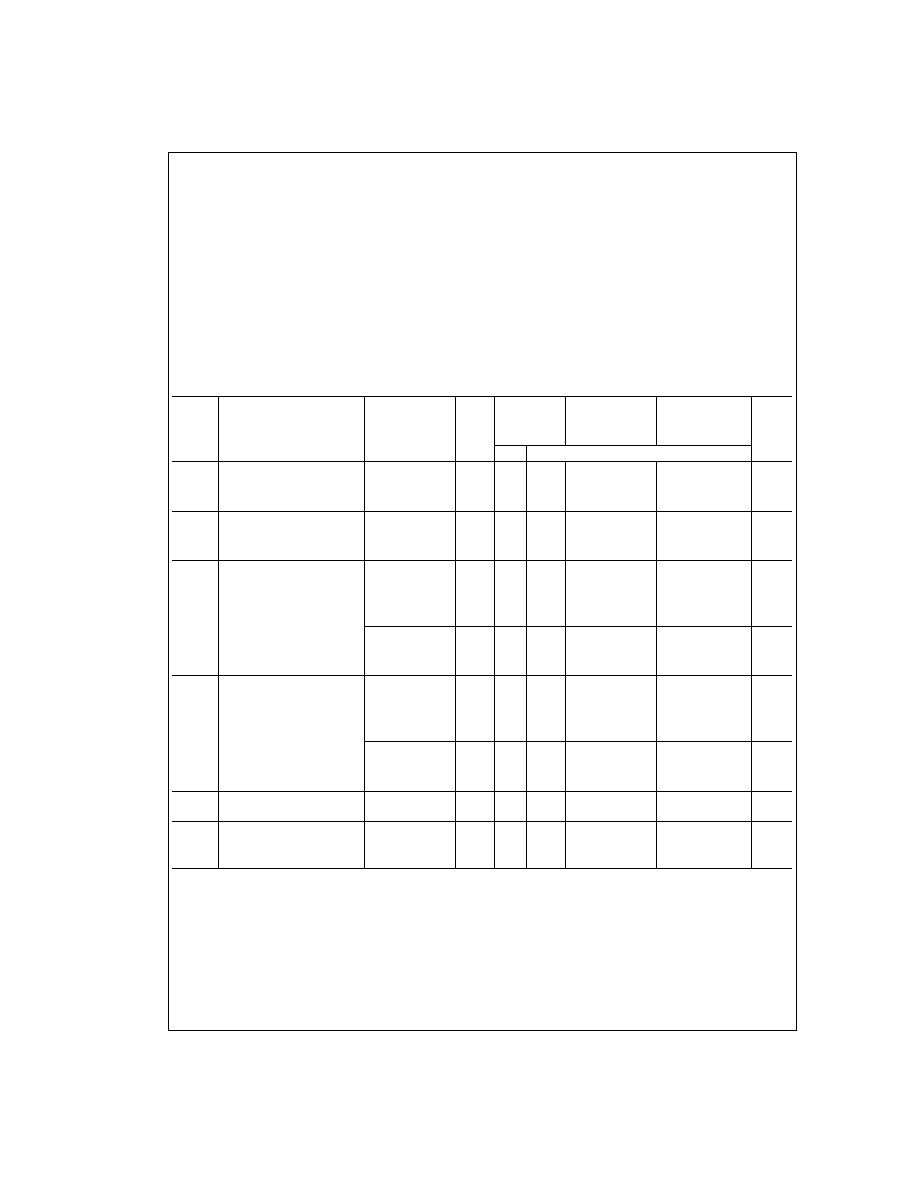
Absolute Maximum Ratings (Notes 2, 1)
Supply Voltage (V
CC)
0.5 to +7.0V
DC Input Voltage (V
IN)
1.5 to V
CC+1.5V
DC Output Voltage (V
OUT)
0.5 to V
CC+0.5V
Clamp Diode Current (I
CD)
±20 mA
DC Output Current, per pin (I
OUT)
±25 mA
DC V
CC or GND Current, per pin (ICC)
±50 mA
Storage Temperature Range (T
STG)
65C to +150C
Power Dissipation (P
D)
(Note 3)
600 mW
S.O. Package only
500 mW
Lead Temperature (T
L)
(Soldering 10 seconds)
260C
Operating Conditions
Min
Max
Units
Supply Voltage (V
CC)2
6
V
DC Input or Output Voltage
0
V
CC
V
(V
IN,VOUT)
Operating Temp. Range (T
A)
MM74HC
40
+85
C
MM54HC
55
+125
C
Input Rise or Fall Times
(t
r,tf)VCC=2.0V
1000
ns
V
CC=4.5V
500
ns
V
CC=6.0V
400
ns
DC Electrical Characteristics (Note 4)
T
A=25C
74HC
54HC
Symbol
Parameter
Conditions
V
CC
T
A=40 to 85C
T
A=55 to
125C
Units
Typ
Guaranteed Limits
V
IH
Minimum High Level Input
2.0V
1.5
V
Voltage
4.5V
3.15
V
6.0V
4.2
V
IL
Maximum Low Level Input
2.0V
0.5
V
Voltage (Note 5)
4.5V
1.35
V
6.0V
1.8
V
OH
Minimum High Level Output
V
IN=VIH or VIL
Voltage
|I
OUT|≤20 A
2.0V
2.0
1.9
V
4.5V
4.5
4.4
V
6.0V
6.0
5.9
V
IN=VIH or VIL
|I
OUT|≤4.0 mA
4.5V
4.2
3.98
3.84
3.7
V
|I
OUT|≤5.2 mA
6.0V
5.7
5.48
5.34
5.2
V
OL
Maximum Low Level Output
V
IN=VIH or VIL
Voltage
|I
OUT|≤20 A
2.0V
0
0.1
V
4.5V
0
0.1
V
6.0V
0
0.1
V
IN=VIH or VIL
|I
OUT|≤4.0 mA
4.5V
0.2
.26
0.33
0.4
V
|I
OUT|≤5.2 mA
6.0V
0.2
.26
0.33
0.4
V
I
IN
Maximum Input Current
V
IN=VCC or
GND
6.0V
±0.1
±1.0
A
I
CC
Maximum Quiescent Supply
V
IN=VCC or
GND
6.0V
8.0
80
160
A
Current
I
OUT=0A
Note 1: Maximum Ratings are those values beyond which damage to the device may occur.
Note 2: Unless otherwise specified all voltages are referenced to ground.
Note 3: Power Dissipation temperature derating — plastic “N” package: 12 mW/C from 65C to 85C; ceramic “J” package: 12 mW/C from 100C to 125C.
Note 4: For a power supply of 5V ±10% the worst case output voltages (VOH, and VOL) occur for HC at 4.5V. Thus the 4.5V values should be used when designing
with this supply. Worst case VIH and VIL occur at VCC=5.5V and 4.5V respectively. (The VIH value at 5.5V is 3.85V.) The worst case leakage current (IIN,ICC, and
IOZ) occur for CMOS at the higher voltage and so the 6.0V values should be used.
Note 5: VIL limits are currently tested at 20% of VCC. The above VIL specification (30% of VCC) will be implemented no later than Q1, CY’89.
www.fairchildsemi.com
2
相关PDF资料 |
PDF描述 |
|---|---|
| MM74HC595WMX | |
| MM74HC597MX | |
| MM74HC597SJX | |
| MM74HCT544J | HCT SERIES, 8-BIT REGISTERED TRANSCEIVER, INVERTED OUTPUT, CDIP24 |
| MM8001 | UHF BAND, Si, NPN, RF SMALL SIGNAL TRANSISTOR, TO-39 |
相关代理商/技术参数 |
参数描述 |
|---|---|
| MM74HC4040J/A+ | 制造商:未知厂家 制造商全称:未知厂家 功能描述:Asynchronous Up Counter |
| MM74HC4040M | 功能描述:计数器移位寄存器 12-Stage Binary Ctr TUBE RoHS:否 制造商:Texas Instruments 计数器类型: 计数顺序:Serial to Serial/Parallel 电路数量:1 封装 / 箱体:SOIC-20 Wide 逻辑系列: 逻辑类型: 输入线路数量:1 输出类型:Open Drain 传播延迟时间:650 ns 最大工作温度:+ 125 C 最小工作温度:- 40 C 封装:Reel |
| MM74HC4040M | 制造商:Fairchild Semiconductor Corporation 功能描述:74HC CMOS SMD 74HC4040 SOIC16 |
| MM74HC4040M/A+ | 制造商:未知厂家 制造商全称:未知厂家 功能描述:Asynchronous Up Counter |
| MM74HC4040M_Q | 功能描述:计数器 IC 12-Stage Binary Ctr TUBE RoHS:否 制造商:NXP Semiconductors 计数器类型:Binary Counters 逻辑系列:74LV 位数:10 计数法: 计数顺序: 工作电源电压:1 V to 5.5 V 工作温度范围:- 40 C to + 125 C 封装 / 箱体:SOT-109 封装:Reel |
发布紧急采购,3分钟左右您将得到回复。