- 您现在的位置:买卖IC网 > PDF目录378673 > MMFT2406T (Motorola, Inc.) MEDIUM POWER TMOS FET 700 mA 240 VOLTS PDF资料下载
参数资料
| 型号: | MMFT2406T |
| 厂商: | Motorola, Inc. |
| 英文描述: | MEDIUM POWER TMOS FET 700 mA 240 VOLTS |
| 中文描述: | 场效应管中功率TMOS是240伏700毫安 |
| 文件页数: | 3/6页 |
| 文件大小: | 90K |
| 代理商: | MMFT2406T |
3
Motorola Small–Signal Transistors, FETs and Diodes Device Data
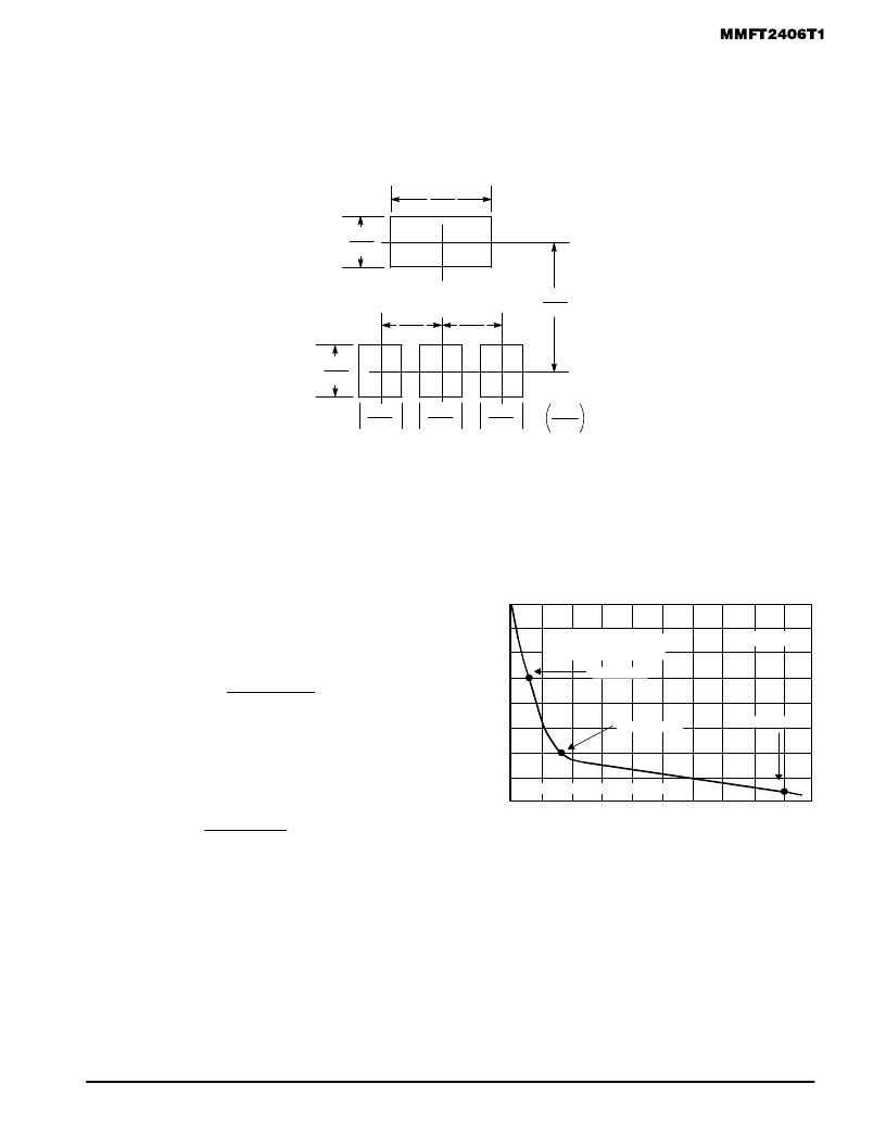
INFORMATION FOR USING THE SOT-223 SURFACE MOUNT PACKAGE
MINIMUM RECOMMENDED FOOTPRINT FOR SURFACE MOUNTED APPLICATIONS
Surface mount board layout is a critical portion of the total
design. The footprint for the semiconductor packages must
be the correct size to insure proper solder connection
interface between the board and the package. With the
correct pad geometry, the packages will self align when
subjected to a solder reflow process.
SOT-223
0.079
2.0
0.15
3.8
0.248
6.3
0.079
2.0
0.059
1.5
0.059
1.5
0.059
1.5
0.091
2.3
0.091
2.3
mm
inches
SOT-223 POWER DISSIPATION
The power dissipation of the SOT-223 is a function of the
pad size. This can vary from the minimum pad size for
soldering to a pad size given for maximum power dissipation.
Power dissipation for a surface mount device is determined
by TJ(max), the maximum rated junction temperature of the
die, R
θ
JA, the thermal resistance from the device junction to
ambient, and the operating temperature, TA. Using the
values provided on the data sheet for the SOT-223 package,
PD can be calculated as follows:
PD =
TJ(max) – TA
R
θ
JA
The values for the equation are found in the maximum
ratings table on the data sheet. Substituting these values into
the equation for an ambient temperature TA of 25
°
C, one can
calculate the power dissipation of the device which in this
case is 1.5 watts.
PD =150
°
C – 25
°
C= 1.5 watts
83.3
°
C/W
The 83.3
°
C/W for the SOT-223 package assumes the use
of the recommended footprint on a glass epoxy printed circuit
board to achieve a power dissipation of 1.5 watts. There are
other alternatives to achieving higher power dissipation from
the SOT-223 package. One is to increase the area of the
collector pad. By increasing the area of the collector pad, the
power dissipation can be increased. Although the power
dissipation can almost be doubled with this method, area is
taken up on the printed circuit board which can defeat the
purpose of using surface mount technology. A graph of R
θ
JA
versus collector pad area is shown in Figure 1.
0.8 Watts
1.25 Watts*
1.5 Watts
R
θ
J
t
°
A, Area (square inches)
0.0
0.2
0.4
0.6
0.8
1.0
160
140
120
100
80
Figure 1. Thermal Resistance versus Collector
Pad Area for the SOT-223 Package (Typical)
Board Material = 0.0625
″
G-10/FR-4, 2 oz Copper
TA = 25
°
C
*Mounted on the DPAK footprint
Another alternative would be to use a ceramic substrate or
an aluminum core board such as Thermal Clad
. Using a
board material such as Thermal Clad, an aluminum core
board, the power dissipation can be doubled using the same
footprint.
相关PDF资料 |
PDF描述 |
|---|---|
| MMFT2955E | TMOS MEDIUM POWER FET 1.2 AMP 60 VOLTS |
| MMFT3055EL | MEDIUM POWER LOGIC LEVEL TMOS FET 1.5 AMP 60 VOLTS |
| MMFT3055VL | TMOS POWER FET 1.5 AMPERES 60 VOLT |
| MMFT3055E | MEDIUM POWER TMOS FET 1.7 AMP 60 VOLTS |
| MMFT3055V | TMOS POWER FET 1.7 AMPERES 60 VOLTS |
相关代理商/技术参数 |
参数描述 |
|---|---|
| MMFT2406T1 | 功能描述:MOSFET N-CH 240V 700MA SOT223 RoHS:否 类别:分离式半导体产品 >> FET - 单 系列:- 标准包装:1,000 系列:MESH OVERLAY™ FET 型:MOSFET N 通道,金属氧化物 FET 特点:逻辑电平门 漏极至源极电压(Vdss):200V 电流 - 连续漏极(Id) @ 25° C:18A 开态Rds(最大)@ Id, Vgs @ 25° C:180 毫欧 @ 9A,10V Id 时的 Vgs(th)(最大):4V @ 250µA 闸电荷(Qg) @ Vgs:72nC @ 10V 输入电容 (Ciss) @ Vds:1560pF @ 25V 功率 - 最大:40W 安装类型:通孔 封装/外壳:TO-220-3 整包 供应商设备封装:TO-220FP 包装:管件 |
| MMFT2406T1G | 制造商:ONSEMI 制造商全称:ON Semiconductor 功能描述:Power MOSFET |
| MMFT2406T3 | 制造商:Rochester Electronics LLC 功能描述: |
| MMFT2406T3G | 制造商:ONSEMI 制造商全称:ON Semiconductor 功能描述:Power MOSFET |
| MMFT2955E | 制造商:MOTOROLA 制造商全称:Motorola, Inc 功能描述:TMOS MEDIUM POWER FET 1.2 AMP 60 VOLTS |
发布紧急采购,3分钟左右您将得到回复。