- 您现在的位置:买卖IC网 > PDF目录378673 > MMFT6N03HD (MOTOROLA INC) TMOS POWER 6.0 AMPERES 30 VOLTS PDF资料下载
参数资料
| 型号: | MMFT6N03HD |
| 厂商: | MOTOROLA INC |
| 元件分类: | 小信号晶体管 |
| 英文描述: | TMOS POWER 6.0 AMPERES 30 VOLTS |
| 中文描述: | 6000 mA, 30 V, N-CHANNEL, Si, SMALL SIGNAL, MOSFET, TO-261AA |
| 文件页数: | 1/4页 |
| 文件大小: | 74K |
| 代理商: | MMFT6N03HD |
1
Motorola, Inc. 1996
Medium Power Surface Mount Products
These medium power SOT–223 devices are an advanced series
of power MOSFETs which utilize Motorola’s High Cell Density
HDTMOS process. These surface mount MOSFETs feature low
RDS(on) and true logic level performance. They are capable of
withstanding high energy in the avalanche and commutation
modes and the drain–to–source diode has a very low reverse
recovery time. SOT–223 HDTMOS devices are designed for use in
low voltage, high speed switching applications where power
efficiency is important. Typical applications are dc–dc converters,
and power management in peripheral products such as printers
and cordless phones. They can also be used for low voltage motor
controls in mass storage products such as disk drives and tape
drives. The avalanche energy is specified to eliminate the
guesswork in designs where inductive loads are switched and offer
additional safety margin against unexpected voltage transients.
Low RDS(on) Provides Higher Efficiency and Extends Battery Life
Logic Level Gate Drive — Can Be Driven by Logic ICs
SOT–223 Saves Board Space and Height
Diode Is Characterized for Use In Bridge Circuits
IDSS Specified at Elevated Temperature
Avalanche Energy Specified
Mounting Information for SOT–223 Package Provided
Use MMFT5N02HDT1 to order the 7 inch/1000 unit reel
Use MMFT5N02HDT3 to order the 13 inch/4000 unit reel
MAXIMUM RATINGS
(TC = 25
°
C unless otherwise noted)
Rating
Symbol
Value
Unit
Drain–to–Source Voltage
VDSS
VDGR
VGS
ID
ID
IDM
PD
30
Vdc
Drain–to–Gate Voltage (RGS = 1.0 M
)
Gate–to–Source Voltage – Continuous
Drain Current – Continuous(1)
Drain Current
– Continuous @ 100
°
C(1)
Drain Current
– Single Pulse (tp
≤
10
μ
s)(1)
Total PD @ TA = 25
°
C(1)
Total PD @ TA = 25
°
C(2)
Operating and Storage Temperature Range
30
Vdc
±
20
6.0
3.7
40
Vdc
Adc
Apk
1.8
0.8
Watts
TJ, Tstg
EAS
–55 to 150
°
C
mJ
Single Pulse Drain–to–Source Avalanche Energy – Starting TJ = 25
°
C
(VDD = 25 Vdc, VGS = 10 Vdc, Peak IL = 6.0 Apk, L = 72 mH)
Thermal Resistance
– Junction to Ambient(1)
– Junction to Ambient(2)
1300
R
θ
JA
R
θ
JA
TL
70
156
°
C/W
Maximum Lead Temperature for Soldering Purposes, 1/8
″
from case for 10 seconds
260
°
C
(1) When mounted on 1” sq. Drain pad on FR–4 bd material
(2) When mounted on minimum recommended Drain pad on FR–4 bd material
This document contains information on a new product. Specifications and information herein are subject to change without notice.
HDTMOS is a trademark of Motorola, Inc. TMOS is a registered trademark of Motorola, Inc.
Order this document through
Power Products Marketing
SEMICONDUCTOR TECHNICAL DATA
TMOS POWER FET
6.0 AMPERES
30 VOLTS
RDS(on) = 0.050 OHM
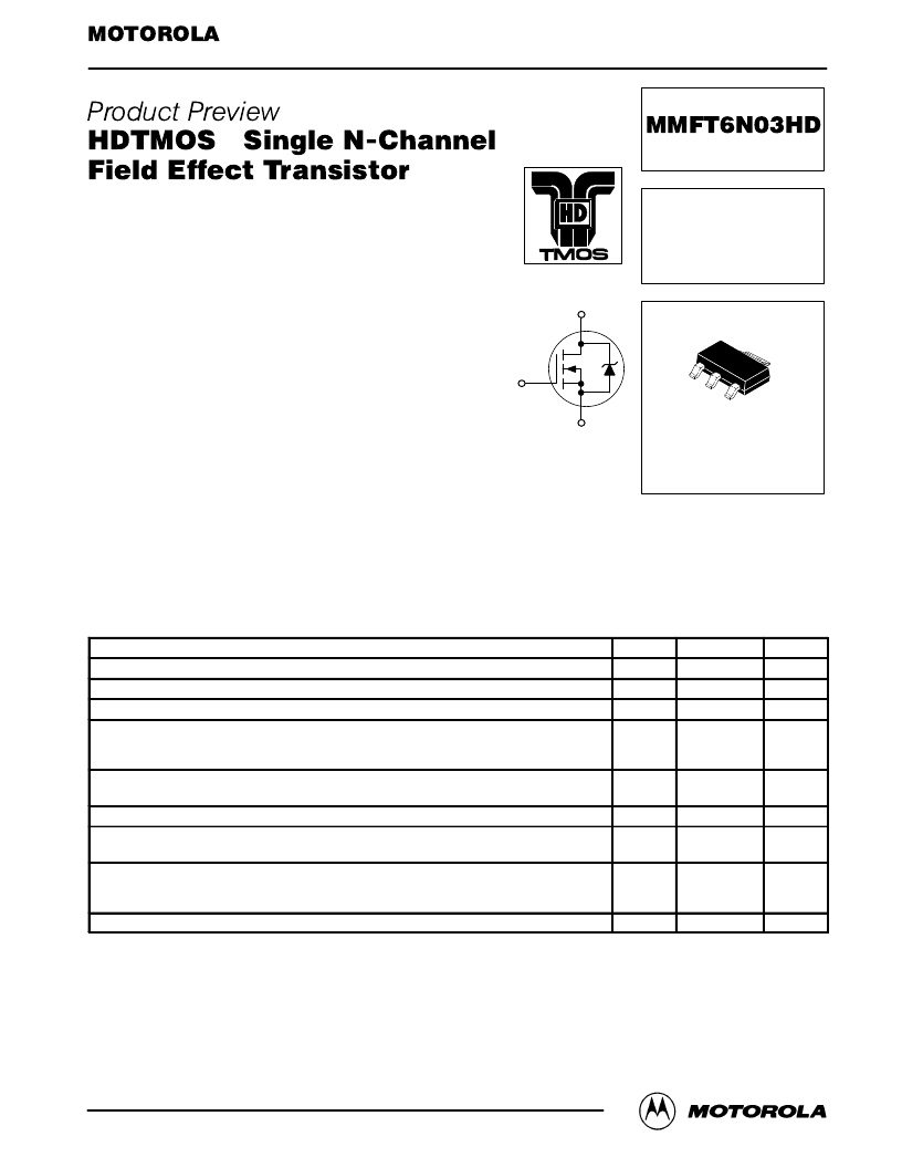
D
S
G
CASE 318E–04, Style 3
TO–261AA
1
2
3
4
相关PDF资料 |
PDF描述 |
|---|---|
| MMFT960T1 | MEDIUM POWER TMOS FET 300 mA 60 VOLTS |
| MMFT960T1 | Power MOSFET 300 mA, 60 Volts |
| MMJT9410 | Bipolar Power Transistors |
| MMJT9435 | Bipolar Power Transistors |
| MMM5063 | Tri-Band GSM GPRS 3.5 V Power Amplifier |
相关代理商/技术参数 |
参数描述 |
|---|---|
| MMFT960T1 | 功能描述:MOSFET 60V 300mA N-Channel RoHS:否 制造商:STMicroelectronics 晶体管极性:N-Channel 汲极/源极击穿电压:650 V 闸/源击穿电压:25 V 漏极连续电流:130 A 电阻汲极/源极 RDS(导通):0.014 Ohms 配置:Single 最大工作温度: 安装风格:Through Hole 封装 / 箱体:Max247 封装:Tube |
| MMFT960T1_06 | 制造商:ONSEMI 制造商全称:ON Semiconductor 功能描述:Power MOSFET 300 mA, 60 Volts N−Channel SOT−223 |
| MMFT960T1G | 功能描述:MOSFET 60V 300mA N-Channel RoHS:否 制造商:STMicroelectronics 晶体管极性:N-Channel 汲极/源极击穿电压:650 V 闸/源击穿电压:25 V 漏极连续电流:130 A 电阻汲极/源极 RDS(导通):0.014 Ohms 配置:Single 最大工作温度: 安装风格:Through Hole 封装 / 箱体:Max247 封装:Tube |
| MMFTN123 | 制造商:Diotec Semiconductor 功能描述: |
| MMFTN138 | 制造商:Diotec 功能描述:Bulk |
发布紧急采购,3分钟左右您将得到回复。