- 您现在的位置:买卖IC网 > PDF目录97608 > MMPQ3906R1 (ON SEMICONDUCTOR) 200 mA, 40 V, 4 CHANNEL, PNP, Si, SMALL SIGNAL TRANSISTOR PDF资料下载
参数资料
| 型号: | MMPQ3906R1 |
| 厂商: | ON SEMICONDUCTOR |
| 元件分类: | 小信号晶体管 |
| 英文描述: | 200 mA, 40 V, 4 CHANNEL, PNP, Si, SMALL SIGNAL TRANSISTOR |
| 封装: | CASE 751B-05, SOP-16 |
| 文件页数: | 3/4页 |
| 文件大小: | 145K |
| 代理商: | MMPQ3906R1 |
MMPQ3906
http://onsemi.com
3
The values for the equation are found in the maximum
ratings table on the data sheet. Substituting these values
into the equation for an ambient temperature TA of 25°C,
one can calculate the power dissipation of the device which
in this case is 1.0 watt.
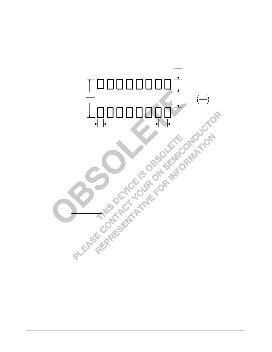
INFORMATION FOR USING THE SO16 SURFACE MOUNT PACKAGE
MINIMUM RECOMMENDED FOOTPRINT FOR SURFACE MOUNTED APPLICATIONS
Surface mount board layout is a critical portion of the to-
tal design. The footprint for the semiconductor packages
must be the correct size to insure proper solder connection
interface between the board and the package. With the cor-
rect pad geometry, the packages will self align when sub-
jected to a solder reflow process.
SO16 POWER DISSIPATION
PD =
TJ(max) TA
RθJA
PD =
150°C 25°C
125°C/W
= 1.0 watt
The power dissipation of the SO16 is a function of the
pad size. This can vary from the minimum pad size for sol-
dering to a pad size given for maximum power dissipation.
Power dissipation for a surface mount device is determined
by TJ(max), the maximum rated junction temperature of the
die, RθJA, the thermal resistance from the device junction
to ambient, and the operating temperature, TA. Using the
values provided on the data sheet for the SO16 package,
PD can be calculated as follows:
The 125°C/W for the SO16 package assumes the use of
the recommended footprint on a glass epoxy printed circuit
board to achieve a power dissipation of 1.0 watt. There are
other alternatives to achieving higher power dissipation
from the SO16 package. Another alternative would be to
use a ceramic substrate or an aluminum core board such as
Thermal Clad. Using a board material such as Thermal
Clad, an aluminum core board, the power dissipation can
be doubled using the same footprint.
SOLDERING PRECAUTIONS
The melting temperature of solder is higher than the
rated temperature of the device. When the entire device is
heated to a high temperature, failure to complete soldering
within a short time could result in device failure. There-
fore, the following items should always be observed in or-
der to minimize the thermal stress to which the devices are
subjected.
Always preheat the device.
The delta temperature between the preheat and solder-
ing should be 100°C or less.*
When preheating and soldering, the temperature of the
leads and the case must not exceed the maximum tem-
perature ratings as shown on the data sheet. When
using infrared heating with the reflow soldering meth-
od, the difference shall be a maximum of 10°C.
The soldering temperature and time shall not exceed
260°C for more than 10 seconds.
When shifting from preheating to soldering, the maxi-
mum temperature gradient shall be 5°C or less.
After soldering has been completed, the device should
be allowed to cool naturally for at least three minutes.
Gradual cooling should be used as the use of forced
cooling will increase the temperature gradient and
result in latent failure due to mechanical stress.
Mechanical stress or shock should not be applied dur-
ing cooling.
* Soldering a device without preheating can cause exces-
sive thermal shock and stress which can result in damage
to the device.
SO16
mm
inches
0.060
1.52
0.275
7.0
0.024
0.6
0.050
1.270
0.155
4.0
相关PDF资料 |
PDF描述 |
|---|---|
| MMPQ3906G | 200 mA, 40 V, 4 CHANNEL, PNP, Si, SMALL SIGNAL TRANSISTOR |
| MMPQ3906R1G | 200 mA, 40 V, 4 CHANNEL, PNP, Si, SMALL SIGNAL TRANSISTOR |
| MMPQ3906R2G | 200 mA, 40 V, 4 CHANNEL, PNP, Si, SMALL SIGNAL TRANSISTOR |
| MMS9014-L | 100 mA, 45 V, NPN, Si, SMALL SIGNAL TRANSISTOR |
| MMS9014-H | 100 mA, 45 V, NPN, Si, SMALL SIGNAL TRANSISTOR |
相关代理商/技术参数 |
参数描述 |
|---|---|
| MMPQ3906R2 | 功能描述:两极晶体管 - BJT 200mA 40V PNP RoHS:否 制造商:STMicroelectronics 配置: 晶体管极性:PNP 集电极—基极电压 VCBO: 集电极—发射极最大电压 VCEO:- 40 V 发射极 - 基极电压 VEBO:- 6 V 集电极—射极饱和电压: 最大直流电集电极电流: 增益带宽产品fT: 直流集电极/Base Gain hfe Min:100 A 最大工作温度: 安装风格:SMD/SMT 封装 / 箱体:PowerFLAT 2 x 2 |
| MMPQ6502 | 制造商:CENTRAL 制造商全称:Central Semiconductor Corp 功能描述:SURFACE MOUNT COMPLEMENTARY SILICON QUAD TRANSISTOR |
| MMPQ6700 | 功能描述:两极晶体管 - BJT NPN/PNP Transistor Gen Purp Quad RoHS:否 制造商:STMicroelectronics 配置: 晶体管极性:PNP 集电极—基极电压 VCBO: 集电极—发射极最大电压 VCEO:- 40 V 发射极 - 基极电压 VEBO:- 6 V 集电极—射极饱和电压: 最大直流电集电极电流: 增益带宽产品fT: 直流集电极/Base Gain hfe Min:100 A 最大工作温度: 安装风格:SMD/SMT 封装 / 箱体:PowerFLAT 2 x 2 |
| MMPQ6700_Q | 功能描述:两极晶体管 - BJT NPN/PNP Transistor Gen Purp Quad RoHS:否 制造商:STMicroelectronics 配置: 晶体管极性:PNP 集电极—基极电压 VCBO: 集电极—发射极最大电压 VCEO:- 40 V 发射极 - 基极电压 VEBO:- 6 V 集电极—射极饱和电压: 最大直流电集电极电流: 增益带宽产品fT: 直流集电极/Base Gain hfe Min:100 A 最大工作温度: 安装风格:SMD/SMT 封装 / 箱体:PowerFLAT 2 x 2 |
| MMPQ6700R1 | 功能描述:两极晶体管 - BJT 200mA 40V Quad RoHS:否 制造商:STMicroelectronics 配置: 晶体管极性:PNP 集电极—基极电压 VCBO: 集电极—发射极最大电压 VCEO:- 40 V 发射极 - 基极电压 VEBO:- 6 V 集电极—射极饱和电压: 最大直流电集电极电流: 增益带宽产品fT: 直流集电极/Base Gain hfe Min:100 A 最大工作温度: 安装风格:SMD/SMT 封装 / 箱体:PowerFLAT 2 x 2 |
发布紧急采购,3分钟左右您将得到回复。