- 您现在的位置:买卖IC网 > PDF目录378673 > MMSF7P03HD (Motorola, Inc.) SINGLE TMOS POWER MOSFET 30 VOLTS PDF资料下载
参数资料
| 型号: | MMSF7P03HD |
| 厂商: | Motorola, Inc. |
| 英文描述: | SINGLE TMOS POWER MOSFET 30 VOLTS |
| 中文描述: | 单任务操作系统功率MOSFET 30伏 |
| 文件页数: | 4/10页 |
| 文件大小: | 214K |
| 代理商: | MMSF7P03HD |
4
Motorola TMOS Power MOSFET Transistor Device Data
POWER MOSFET SWITCHING
Switching behavior is most easily modeled and predicted
by recognizing that the power MOSFET is charge controlled.
The lengths of various switching intervals (
t) are deter-
mined by how fast the FET input capacitance can be charged
by current from the generator.
The published capacitance data is difficult to use for calculat-
ing rise and fall because drain–gate capacitance varies
greatly with applied voltage. Accordingly, gate charge data is
used. In most cases, a satisfactory estimate of average input
current (IG(AV)) can be made from a rudimentary analysis of
the drive circuit so that
t = Q/IG(AV)
During the rise and fall time interval when switching a resis-
tive load, VGS remains virtually constant at a level known as
the plateau voltage, VSGP. Therefore, rise and fall times may
be approximated by the following:
tr = Q2 x RG/(VGG – VGSP)
tf = Q2 x RG/VGSP
where
VGG = the gate drive voltage, which varies from zero to VGG
RG = the gate drive resistance
and Q2 and VGSP are read from the gate charge curve.
During the turn–on and turn–off delay times, gate current is
not constant. The simplest calculation uses appropriate val-
ues from the capacitance curves in a standard equation for
voltage change in an RC network. The equations are:
td(on) = RG Ciss In [VGG/(VGG – VGSP)]
td(off) = RG Ciss In (VGG/VGSP)
The capacitance (Ciss) is read from the capacitance curve at
a voltage corresponding to the off–state condition when cal-
culating td(on) and is read at a voltage corresponding to the
on–state when calculating td(off).
At high switching speeds, parasitic circuit elements com-
plicate the analysis. The inductance of the MOSFET source
lead, inside the package and in the circuit wiring which is
common to both the drain and gate current paths, produces a
voltage at the source which reduces the gate drive current.
The voltage is determined by Ldi/dt, but since di/dt is a func-
tion of drain current, the mathematical solution is complex.
The MOSFET output capacitance also complicates the
mathematics. And finally, MOSFETs have finite internal gate
resistance which effectively adds to the resistance of the
driving source, but the internal resistance is difficult to mea-
sure and, consequently, is not specified.
The resistive switching time variation versus gate resis-
tance (Figure 9) shows how typical switching performance is
affected by the parasitic circuit elements. If the parasitics
were not present, the slope of the curves would maintain a
value of unity regardless of the switching speed. The circuit
used to obtain the data is constructed to minimize common
inductance in the drain and gate circuit loops and is believed
readily achievable with board mounted components. Most
power electronic loads are inductive; the data in the figure is
taken with a resistive load, which approximates an optimally
snubbed inductive load. Power MOSFETs may be safely op-
erated into an inductive load; however, snubbing reduces
switching losses.
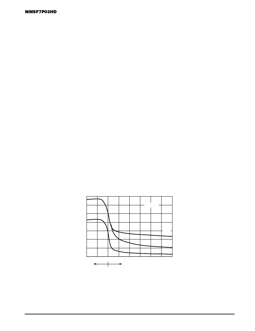
Figure 7. Capacitance Variation
10
30
–10
VDS, DRAIN–TO–SOURCE VOLTAGE (VOLTS)
3500
1000
C
500
0
0
Ciss
Crss
Coss
TJ = 25
°
C
VGS
VDS
20
1500
2000
2500
3000
相关PDF资料 |
PDF描述 |
|---|---|
| MMT3823 | JUNCTION FIELD EFFECT TRANSISTOR |
| MMT4261 | RF TRANSISTOR |
| MMT72 | NPN SWITCHING TRANSISTOR |
| MMT74 | RF AMPLIFIER TRANSISTOR |
| MMT918 | NPN VHF/UHF TRANSISTOR |
相关代理商/技术参数 |
参数描述 |
|---|---|
| MMSF7P03HDR2 | 功能描述:MOSFET 30V 7A P-Channel RoHS:否 制造商:STMicroelectronics 晶体管极性:N-Channel 汲极/源极击穿电压:650 V 闸/源击穿电压:25 V 漏极连续电流:130 A 电阻汲极/源极 RDS(导通):0.014 Ohms 配置:Single 最大工作温度: 安装风格:Through Hole 封装 / 箱体:Max247 封装:Tube |
| MMSF7P03HDR2G | 功能描述:MOSFET PFET SO8S 30V 7A 35mOhm RoHS:否 制造商:STMicroelectronics 晶体管极性:N-Channel 汲极/源极击穿电压:650 V 闸/源击穿电压:25 V 漏极连续电流:130 A 电阻汲极/源极 RDS(导通):0.014 Ohms 配置:Single 最大工作温度: 安装风格:Through Hole 封装 / 箱体:Max247 封装:Tube |
| MM-SIO-R-01 | 功能描述:单板计算机 MiniModule Super I/O for CM 730 Legacy IO RoHS:否 制造商:Ampro By ADLINK 外观尺寸:EPIC 处理器类型:Intel Atom D510 频率:1.66 GHz 存储容量:2 GB (max) 存储类型:DDR2, L2 Cache 接口类型:Ethernet, PS/2, SATA, Serial, USB 工作电源电压:5 V, 12 V 功耗:13 W 最大工作温度:+ 70 C 尺寸:165.1 mm x 114.3 mm |
| MMSKG1 | 制造商:Siemens 功能描述: |
| MMSL101 | 制造商:Preh Elec. 功能描述: |
发布紧急采购,3分钟左右您将得到回复。