- 您现在的位置:买卖IC网 > PDF目录80528 > MPC5566MVR144 (FREESCALE SEMICONDUCTOR INC) 32-BIT, FLASH, 114 MHz, MICROCONTROLLER, PBGA416 PDF资料下载
参数资料
| 型号: | MPC5566MVR144 |
| 厂商: | FREESCALE SEMICONDUCTOR INC |
| 元件分类: | 微控制器/微处理器 |
| 英文描述: | 32-BIT, FLASH, 114 MHz, MICROCONTROLLER, PBGA416 |
| 封装: | 27 X 27 MM, 1 MM PITCH, LEAD FREE, PLASTIC, MS-034AAL-1, BGA-416 |
| 文件页数: | 8/66页 |
| 文件大小: | 1351K |
| 代理商: | MPC5566MVR144 |
第1页第2页第3页第4页第5页第6页第7页当前第8页第9页第10页第11页第12页第13页第14页第15页第16页第17页第18页第19页第20页第21页第22页第23页第24页第25页第26页第27页第28页第29页第30页第31页第32页第33页第34页第35页第36页第37页第38页第39页第40页第41页第42页第43页第44页第45页第46页第47页第48页第49页第50页第51页第52页第53页第54页第55页第56页第57页第58页第59页第60页第61页第62页第63页第64页第65页第66页
MPC5566 Microcontroller Data Sheet, Rev. 2.0
Electrical Characteristics
Freescale Semiconductor
16
40
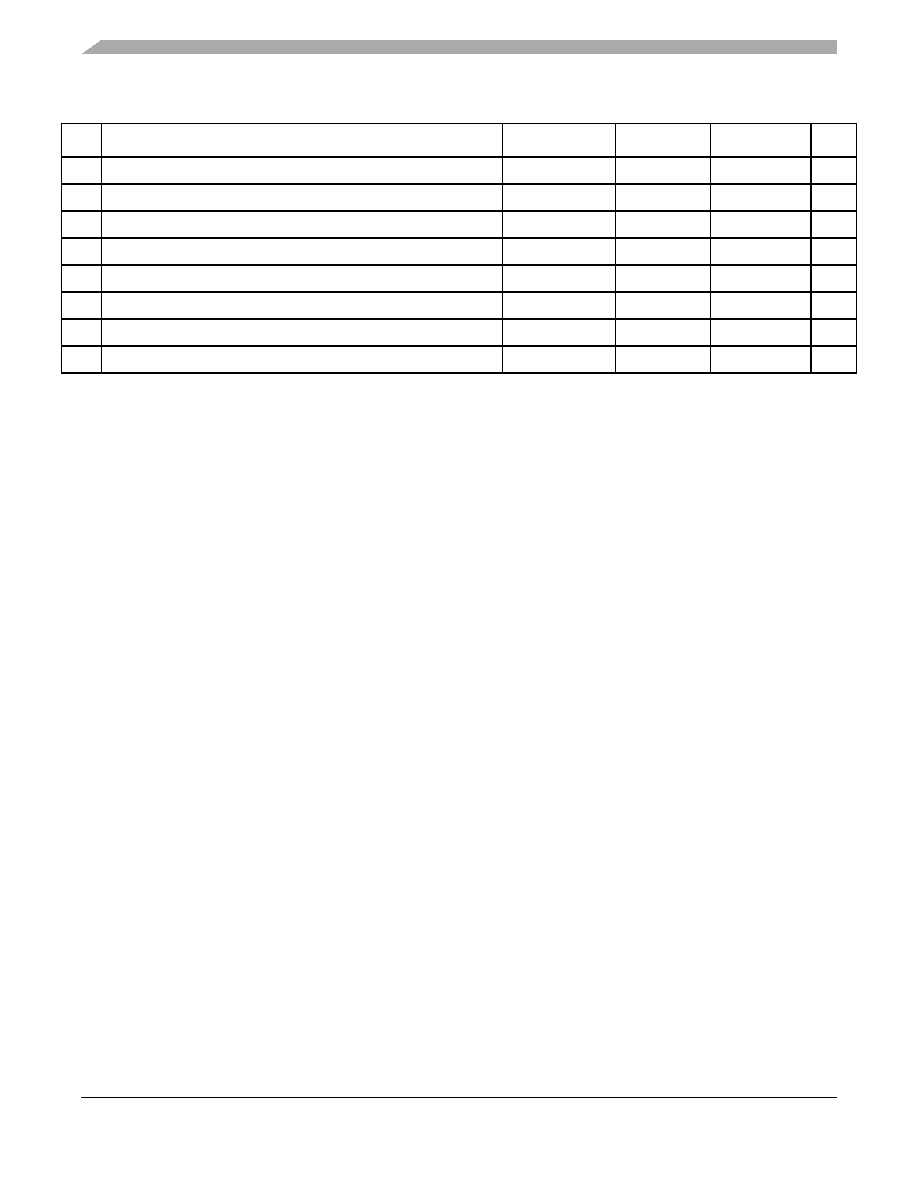
VREF differential voltage
VRH – VRL
4.5
5.25
V
41
VSSSYN to VSS differential voltage
VSSSYN – VSS
–50
50
mV
42
VRCVSS to VSS differential voltage
VRCVSS – VSS
–50
50
mV
43
VDDF to VDD differential voltage
VDDF – VDD
–100
100
mV
43a VRC33 to VDDSYN differential voltage
VRC33 – VDDSYN
–0.1
0.1 19
V
44
Analog input differential signal range (with common mode 2.5 V)
VIDIFF
–2.5
2.5
V
45
Operating temperature range, ambient (packaged)
TA = (TL to TH)TL
TH
οC
46
Slew rate on power-supply pins
—
50
V/ms
1 V
DDE2 and VDDE3 are limited to 2.25–3.6 V only if EBTS = 0; VDDE2 and VDDE3 have a range of 1.6–3.6 V if EBTS = 1.
2 | V
DDA0 – VDDA1 | must be < 0.1 V.
3 V
PP can drop to 3.0 V during read operations.
4 If standby operation is not required, connect V
STBY to ground.
5 Applies to CLKOUT, external bus pins, and Nexus pins.
6 Maximum average RMS DC current.
7 Eight-way cache enabled (L1CSR0[CORG] = 0b0).
8 Average current measured on automotive benchmark.
9 Peak currents can be higher on specialized code.
10 High use current measured while running optimized SPE assembly code with all code and data 100% locked in cache
(0% miss rate) with all channels of the eMIOS and eTPU running autonomously, plus the eDMA transferring data continuously from
SRAM to SRAM. Higher currents are possible if an ‘idle’ loop that crosses cache lines is run from cache. Write code to avoid this
condition.
11 Four-way cache enabled (L1CSR0[CORG] = 0b1) or (L1CSR0[CORG] = 0b0 with L1CSR0[WAM] = 0b1, L1CSR0[WID] = 0b1111,
L1CSR0[WDD] = 0b1111, L1CSR0[AWID] = 0b1, and L1CSR0[AWDD] = 0b1).
12 Figure 3 shows an illustration of the I
DD_STBY values interpolated for these temperature values.
13 Power requirements for the V
DD33 supply depend on the frequency of operation, load of all I/O pins, and the voltages on the I/O
segments. Refer to Table 11 for values to calculate the power dissipation for a specific operation.
14 Power requirements for each I/O segment are dependent on the frequency of operation and load of the I/O pins on a particular I/O
segment, and the voltage of the I/O segment. Refer to Table 10 for values to calculate power dissipation for specific operation. The
total power consumption of an I/O segment is the sum of the individual power consumptions for each pin on the segment.
15 Absolute value of current, measured at V
IL and VIH.
16 Weak pullup/down inactive. Measured at V
DDE = 3.6 V and VDDEH = 5.25 V. Applies to pad types: pad_fc, pad_sh, and pad_mh.
17 Maximum leakage occurs at maximum operating temperature. Leakage current decreases by approximately one-half for each 8 oC
to 12 oC, in the ambient temperature range of 50 oC to 125 oC. Applies to pad types: pad_a and pad_ae.
18 V
SSA refers to both VSSA0 and VSSA1. | VSSA0 – VSSA1 | must be < 0.1 V.
19 Up to 0.6 V during power up and power down.
Table 9. DC Electrical Specifications (TA = TL – TH) (continued)
Spec
Characteristic
Symbol
Min
Max
Unit
Because
of
an
order
from
the
United
States
International
Trade
Commission,
BGA-packaged
product
lines
and
part
numbers
indicated
here
currently
are
not
available
from
Freescale
for
import
or
sale
in
the
United
States
prior
to
September
2010:
MPC551x
and
MPC5533
products
in
208
MAPBGA
packages;
MPC5534
and
MPC5553
products
in
208
and
496
MAPBGA
packages;
MPC5554,
MPC5565,
MPC5566
and
MPC5567
products
in
496
MAPBGA
packages
相关PDF资料 |
PDF描述 |
|---|---|
| MCF54453CVR200 | 32-BIT, 200 MHz, RISC PROCESSOR, PBGA360 |
| MC9S12XF128J0MLMR | MICROCONTROLLER, PQFP112 |
| MPC8555ECVTAKD | RISC PROCESSOR, PBGA783 |
| MPC8572CPXAUNB | 32-BIT, 1333 MHz, MICROPROCESSOR, PBGA1023 |
| MPC8572CVTATNB | 32-BIT, 1200 MHz, MICROPROCESSOR, PBGA1023 |
相关代理商/技术参数 |
参数描述 |
|---|---|
| MPC5566MZP132 | 功能描述:32位微控制器 - MCU 3M FLASH,32K CACHE 128K RoHS:否 制造商:Texas Instruments 核心:C28x 处理器系列:TMS320F28x 数据总线宽度:32 bit 最大时钟频率:90 MHz 程序存储器大小:64 KB 数据 RAM 大小:26 KB 片上 ADC:Yes 工作电源电压:2.97 V to 3.63 V 工作温度范围:- 40 C to + 105 C 封装 / 箱体:LQFP-80 安装风格:SMD/SMT |
| MPC5566MZP132R | 制造商:Freescale Semiconductor 功能描述:32-BIT MPC55XX POWERPC RISC 3MB FLASH 1.8V/2.5V/3.3V/5V 416 - Tape and Reel |
| MPC5566MZP144 | 功能描述:32位微控制器 - MCU 3M FLASH32K CACHE 128K RoHS:否 制造商:Texas Instruments 核心:C28x 处理器系列:TMS320F28x 数据总线宽度:32 bit 最大时钟频率:90 MHz 程序存储器大小:64 KB 数据 RAM 大小:26 KB 片上 ADC:Yes 工作电源电压:2.97 V to 3.63 V 工作温度范围:- 40 C to + 105 C 封装 / 箱体:LQFP-80 安装风格:SMD/SMT |
| MPC5567 | 制造商:FREESCALE 制造商全称:Freescale Semiconductor, Inc 功能描述:Microcontroller |
| MPC5567EVB | 功能描述:BOARD EVALUATION MPC5567MZP132 RoHS:否 类别:编程器,开发系统 >> 过时/停产零件编号 系列:- 标准包装:1 系列:- 传感器类型:CMOS 成像,彩色(RGB) 传感范围:WVGA 接口:I²C 灵敏度:60 fps 电源电压:5.7 V ~ 6.3 V 嵌入式:否 已供物品:成像器板 已用 IC / 零件:KAC-00401 相关产品:4H2099-ND - SENSOR IMAGE WVGA COLOR 48-PQFP4H2094-ND - SENSOR IMAGE WVGA MONO 48-PQFP |
发布紧急采购,3分钟左右您将得到回复。