- 您现在的位置:买卖IC网 > PDF目录45353 > MPC7410RX400LD (FREESCALE SEMICONDUCTOR INC) 32-BIT, 400 MHz, RISC PROCESSOR, CBGA360 PDF资料下载
参数资料
| 型号: | MPC7410RX400LD |
| 厂商: | FREESCALE SEMICONDUCTOR INC |
| 元件分类: | 微控制器/微处理器 |
| 英文描述: | 32-BIT, 400 MHz, RISC PROCESSOR, CBGA360 |
| 封装: | 25 X 25 MM, 3.20 MM HEIGHT, 1.27 MM PITCH, CERAMIC, BGA-360 |
| 文件页数: | 6/56页 |
| 文件大小: | 864K |
| 代理商: | MPC7410RX400LD |
第1页第2页第3页第4页第5页当前第6页第7页第8页第9页第10页第11页第12页第13页第14页第15页第16页第17页第18页第19页第20页第21页第22页第23页第24页第25页第26页第27页第28页第29页第30页第31页第32页第33页第34页第35页第36页第37页第38页第39页第40页第41页第42页第43页第44页第45页第46页第47页第48页第49页第50页第51页第52页第53页第54页第55页第56页
MPC7410 RISC Microprocessor Hardware Specifications, Rev. 6.1
14
Freescale Semiconductor
Electrical and Thermal Characteristics
4.2.1
Clock AC Specifications
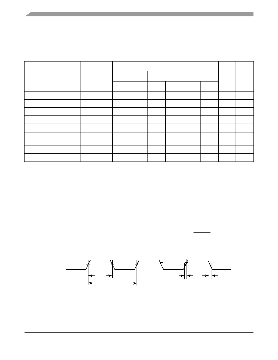
Figure 3 provides the SYSCLK input timing diagram.
Figure 3. SYSCLK Input Timing Diagram
Table 7. Clock AC Timing Specifications
At recommended operating conditions (see Table 3)
Characteristic
Symbol
Maximum Processor Core Frequency
Unit
Notes
400 MHz
450 MHz
500 MHz
Min
Max
Min
Max
Min
Max
Processor frequency
fcore
350
400
350
450
350
500
MHz
1
VCO frequency
fVCO
700
800
700
900
700
1000
MHz
1
SYSCLK frequency
fSYSCLK
33
133
33
133
33
133
MHz
1
SYSCLK cycle time
tSYSCLK
7.5
30
7.5
30
7.5
30
ns
—
SYSCLK rise and fall time
tKR and tKF
—
0.5
—
0.5
—
0.5
ns/V
2
SYSCLK duty cycle
measured at OVDD/2
tKHKL/tSYSCLK
40
60
40
60
40
60
%
3
SYSCLK jitter
—
±150
—
±150
—
±150
ps
4
Internal PLL-relock time
—
100
—
100
—
100
μs5
Notes:
1. Caution: The SYSCLK frequency and PLL_CFG[0:3] settings must be chosen such that the resulting SYSCLK (bus)
frequency, CPU (core) frequency, and PLL (VCO) frequency do not exceed their respective maximum or minimum operating
frequencies. Refer to the PLL_CFG[0:3] signal description in Section 8.1, “PLL Configuration,” for valid PLL_CFG[0:3]
settings.
2. Rise and fall times measurement are determined by the slew rates of the bus interface, rather than by time. As a result, the
0.5 ns rise/fall time spec of the 1.8- and 2.5-V bus interfaces is equivalent to the 1 ns rise/fall time of the 3.3-V bus interface.
Both interfaces required a 2 V/ns slew rate. The slew rate is measured as a 1-V change (from 0.2 to 1.2 V) in 0.5 ns for the
1.8- and 2.5-V bus interfaces, whereas the 3.3-V bus interface required a 2-V change (from 0.4 to 2.4 V) in 1 ns.
3. Timing is guaranteed by design and characterization.
4. This represents total input jitter—short- and long-term combined—and is guaranteed by design.
5. Relock timing is guaranteed by design and characterization. PLL-relock time is the maximum amount of time required for PLL
lock after a stable VDD and SYSCLK are reached during the power-on reset sequence. This specification also applies when
the PLL has been disabled and subsequently re-enabled during sleep mode. Also note that HRESET must be held asserted
for a minimum of 255 bus clocks after the PLL-relock time during the power-on reset sequence.
SYSCLK
VM
CVIH
CVIL
VM = Midpoint Voltage (OVDD/2)
tSYSCLK
tKR
tKF
tKHKL
相关PDF资料 |
PDF描述 |
|---|---|
| MPC7410VS450LE | 32-BIT, 450 MHz, RISC PROCESSOR, CBGA360 |
| MPC7410RX400LE | 32-BIT, 400 MHz, RISC PROCESSOR, CBGA360 |
| MPC745BPX400LE | 32-BIT, 400 MHz, RISC PROCESSOR, PBGA255 |
| MPC745BPX350LE | 32-BIT, 350 MHz, RISC PROCESSOR, PBGA255 |
| MPC755BRX400LE | 32-BIT, 400 MHz, RISC PROCESSOR, CBGA360 |
相关代理商/技术参数 |
参数描述 |
|---|---|
| MPC7410RX400LE | 功能描述:微处理器 - MPU REV 1.4 1.8+/-.05V 105C RoHS:否 制造商:Atmel 处理器系列:SAMA5D31 核心:ARM Cortex A5 数据总线宽度:32 bit 最大时钟频率:536 MHz 程序存储器大小:32 KB 数据 RAM 大小:128 KB 接口类型:CAN, Ethernet, LIN, SPI,TWI, UART, USB 工作电源电压:1.8 V to 3.3 V 最大工作温度:+ 85 C 安装风格:SMD/SMT 封装 / 箱体:FBGA-324 |
| MPC7410RX400NE | 制造商:FREESCALE 制造商全称:Freescale Semiconductor, Inc 功能描述:MPC7410 RISC Microprocessor Hardware Specifications Addendum |
| MPC7410RX450NE | 制造商:FREESCALE 制造商全称:Freescale Semiconductor, Inc 功能描述:MPC7410 RISC Microprocessor Hardware Specifications Addendum |
| MPC7410RX500LE | 功能描述:IC MPU 32BIT 500MHZ PPC 360-CBGA RoHS:否 类别:集成电路 (IC) >> 嵌入式 - 微处理器 系列:MPC74xx 标准包装:2 系列:MPC8xx 处理器类型:32-位 MPC8xx PowerQUICC 特点:- 速度:133MHz 电压:3.3V 安装类型:表面贴装 封装/外壳:357-BBGA 供应商设备封装:357-PBGA(25x25) 包装:托盘 |
| MPC7410THX400LE | 功能描述:微处理器 - MPU NT HITCE RV1.4 1.8V -40C RoHS:否 制造商:Atmel 处理器系列:SAMA5D31 核心:ARM Cortex A5 数据总线宽度:32 bit 最大时钟频率:536 MHz 程序存储器大小:32 KB 数据 RAM 大小:128 KB 接口类型:CAN, Ethernet, LIN, SPI,TWI, UART, USB 工作电源电压:1.8 V to 3.3 V 最大工作温度:+ 85 C 安装风格:SMD/SMT 封装 / 箱体:FBGA-324 |
发布紧急采购,3分钟左右您将得到回复。