- 您现在的位置:买卖IC网 > PDF目录69036 > MPC7410RX500LX (MOTOROLA INC) 32-BIT, 500 MHz, RISC PROCESSOR, CBGA360 PDF资料下载
参数资料
| 型号: | MPC7410RX500LX |
| 厂商: | MOTOROLA INC |
| 元件分类: | 微控制器/微处理器 |
| 英文描述: | 32-BIT, 500 MHz, RISC PROCESSOR, CBGA360 |
| 封装: | 25 X 25 MM, 3.20 MM HEIGHT, 1.27 MM PITCH, CERAMIC, BGA-360 |
| 文件页数: | 19/44页 |
| 文件大小: | 885K |
| 代理商: | MPC7410RX500LX |
第1页第2页第3页第4页第5页第6页第7页第8页第9页第10页第11页第12页第13页第14页第15页第16页第17页第18页当前第19页第20页第21页第22页第23页第24页第25页第26页第27页第28页第29页第30页第31页第32页第33页第34页第35页第36页第37页第38页第39页第40页第41页第42页第43页第44页
26
MPC7410 RISC Microprocessor Hardware Specifications
PRELIMINARY—SUBJECT TO CHANGE WITHOUT NOTICE
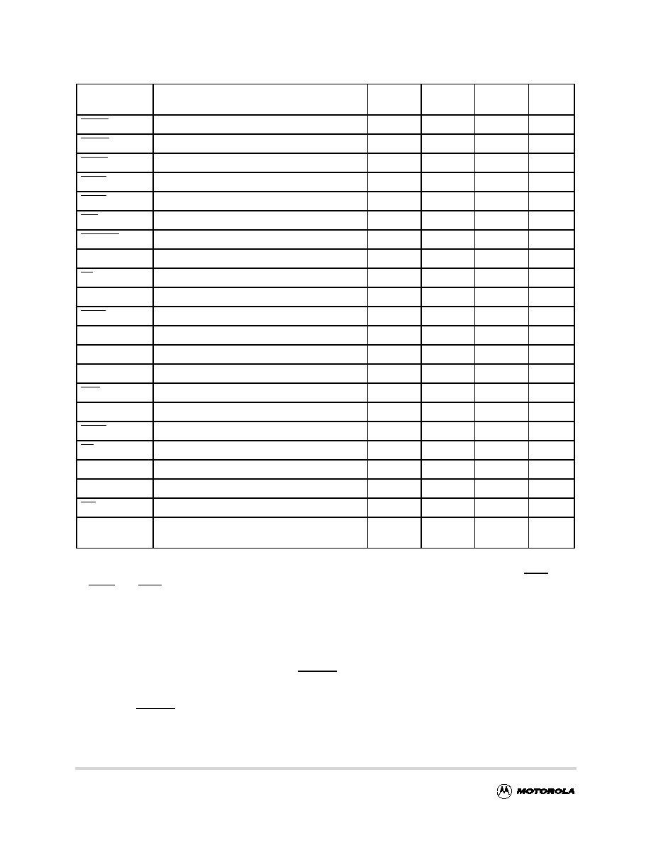
Pinout Listings
Notes:
1. OVdd supplies power to the processor bus, JTAG, and all control signals except the L2 cache controls (L2CE,
L2WE, and L2ZZ); L2OVDD supplies power to the L2 cache interface (L2ADDR[0:18], L2DATA[0:63], L2DP[0:7],
and L2SYNC-OUT) and the L2 control signals; and Vdd supplies power to the processor core and the PLL and DLL
(after filtering to become AVDD and L2AVDD, respectively). These columns serve as a reference for the nominal
voltage supported on a given signal as selected by the BVSEL/L2VSEL pin configurations of Table 2 and the
2. These are test signals for factory use only and must be pulled up to OVdd for normal machine operation.
3. To allow for future I/O voltage changes, provide the option to connect BVSEL and L2VSEL independently to either
OVDD (selects 2.5 V), GND (selects 1.8 V), or to HRESET (selects 2.5 V). For the MPC7410 both the L2 bus and
the processor bus only support the 2.5 V and 1.8 V options. The default selection if BVSEL and/or L2VSEL is left
unconnected is 2.5 V operation.
4. Connect to HRESET to trigger post power-on-reset (por) internal memory test.
5. Ignored in 60x bus mode.
6. Unused output in 60x bus mode.
QACK
B2
Low
Input
BVSEL
QREQ
J3
Low
Output
BVSEL
RSRV
D3
Low
Output
BVSEL
SHD0
B3
Low
I/O
BVSEL
8
SHD1
B4
Low
I/O
BVSEL
5, 8
SMI
A12
Low
Input
BVSEL
SRESET
E10
Low
Input
BVSEL
SYSCLK
H9
—
Input
BVSEL
TA
F1
Low
Input
BVSEL
TBEN
A2
High
Input
BVSEL
TBST
A11
Low
Output
BVSEL
TCK
B10
High
Input
BVSEL
TDI
B7
High
Input
BVSEL
9
TDO
D9
High
Output
BVSEL
TEA
J1
Low
Input
BVSEL
TMS
C8
High
Input
BVSEL
9
TRST
A10
Low
Input
BVSEL
9, 14
TS
K7
Low
I/O
BVSEL
TSIZ[0:2]
A9, B9, C9
High
Output
BVSEL
TT[0:4]
C10, D11, B12, C12, F11
High
I/O
BVSEL
WT
C3
Low
I/O
BVSEL
VDD
G8, G10, G12, J8, J10, J12, L8, L10, L12, N8,
N10, N12
——
N/A
Table 13. Pinout Listing for the MPC7410, 360 CBGA Package (Continued)
Signal Name
Pin Number
Active
I/O
I/F
Select1
Notes
相关PDF资料 |
PDF描述 |
|---|---|
| MPC7410RX450LX | 32-BIT, 450 MHz, RISC PROCESSOR, CBGA360 |
| MPC8241LZP200X | 32-BIT, 200 MHz, RISC PROCESSOR, PBGA357 |
| MPC8245LZU350B | 32-BIT, 350 MHz, RISC PROCESSOR, PBGA352 |
| MPC8245LZU333B | 32-BIT, 333 MHz, RISC PROCESSOR, PBGA352 |
| MPC8245LZU300B | 32-BIT, 300 MHz, RISC PROCESSOR, PBGA352 |
相关代理商/技术参数 |
参数描述 |
|---|---|
| MPC7410THX400LE | 功能描述:微处理器 - MPU NT HITCE RV1.4 1.8V -40C RoHS:否 制造商:Atmel 处理器系列:SAMA5D31 核心:ARM Cortex A5 数据总线宽度:32 bit 最大时钟频率:536 MHz 程序存储器大小:32 KB 数据 RAM 大小:128 KB 接口类型:CAN, Ethernet, LIN, SPI,TWI, UART, USB 工作电源电压:1.8 V to 3.3 V 最大工作温度:+ 85 C 安装风格:SMD/SMT 封装 / 箱体:FBGA-324 |
| MPC7410THX400NE | 制造商:Freescale Semiconductor 功能描述:MPU MPC74XX RISC 64BIT 0.18UM 400MHZ 1.8V/2.5V/3.3V 360FCCBG - Bulk |
| MPC7410THX450NE | 功能描述:微处理器 - MPU NT NITCE RV1.4,1.8V -40C RoHS:否 制造商:Atmel 处理器系列:SAMA5D31 核心:ARM Cortex A5 数据总线宽度:32 bit 最大时钟频率:536 MHz 程序存储器大小:32 KB 数据 RAM 大小:128 KB 接口类型:CAN, Ethernet, LIN, SPI,TWI, UART, USB 工作电源电压:1.8 V to 3.3 V 最大工作温度:+ 85 C 安装风格:SMD/SMT 封装 / 箱体:FBGA-324 |
| MPC7410THX500LE | 功能描述:微处理器 - MPU NT HITCE RV1.4 1.8V -40C RoHS:否 制造商:Atmel 处理器系列:SAMA5D31 核心:ARM Cortex A5 数据总线宽度:32 bit 最大时钟频率:536 MHz 程序存储器大小:32 KB 数据 RAM 大小:128 KB 接口类型:CAN, Ethernet, LIN, SPI,TWI, UART, USB 工作电源电压:1.8 V to 3.3 V 最大工作温度:+ 85 C 安装风格:SMD/SMT 封装 / 箱体:FBGA-324 |
| MPC7410TRX400NE | 制造商:FREESCALE 制造商全称:Freescale Semiconductor, Inc 功能描述:RISC Microprocessor Hardware Specifications Addendum |
发布紧急采购,3分钟左右您将得到回复。