- 您现在的位置:买卖IC网 > PDF目录132964 > MPC7410TRX500LE (MOTOROLA INC) 32-BIT, 500 MHz, RISC PROCESSOR, CBGA360 PDF资料下载
参数资料
| 型号: | MPC7410TRX500LE |
| 厂商: | MOTOROLA INC |
| 元件分类: | 微控制器/微处理器 |
| 英文描述: | 32-BIT, 500 MHz, RISC PROCESSOR, CBGA360 |
| 封装: | 25 X 25 MM, 3.20 MM HEIGHT, 1.27 MM PITCH, CERAMIC, BGA-360 |
| 文件页数: | 10/73页 |
| 文件大小: | 929K |
| 代理商: | MPC7410TRX500LE |
第1页第2页第3页第4页第5页第6页第7页第8页第9页当前第10页第11页第12页第13页第14页第15页第16页第17页第18页第19页第20页第21页第22页第23页第24页第25页第26页第27页第28页第29页第30页第31页第32页第33页第34页第35页第36页第37页第38页第39页第40页第41页第42页第43页第44页第45页第46页第47页第48页第49页第50页第51页第52页第53页第54页第55页第56页第57页第58页第59页第60页第61页第62页第63页第64页第65页第66页第67页第68页第69页第70页第71页第72页第73页
18
MPC7410 RISC Microprocessor Hardware Specications
MOTOROLA
Electrical and Thermal Characteristics
1.4.2.3
L2 Clock AC Specications
The L2CLK frequency is programmed by the L2 Conguration Register (L2CR[4:6]) core-to-L2 divisor
ratio. See Table 14 for example core and L2 frequencies at various divisors. Table 9 provides the potential
range of L2CLK output AC timing specications as dened in Figure 7.
The L2SYNC_OUT signal is intended to be routed halfway out to the SRAMs and then returned to the
L2SYNC_IN input of the MPC7410 to synchronize L2CLK_OUT at the SRAM with the processor’s
internal clock. L2CLK_OUT at the SRAM can be offset forward or backward in time by shortening or
lengthening the routing of L2SYNC_OUT to L2SYNC_IN. See Motorola Application Note AN1794/D,
Backside L2 Timing Analysis for the PCB Design Engineer.
The minimum L2CLK frequency in Table 9 is specied by the maximum delay of the internal DLL. The
variable-tap DLL introduces up to a full clock period delay in the L2CLK_OUTA, L2CLK_OUTB, and
L2SYNC_OUT signals so that the returning L2SYNC_IN signal is phase-aligned with the next core clock
(divided by the L2 divisor ratio). Do not choose a core-to-L2 divisor which results in an L2 frequency below
this minimum, or the L2CLK_OUT signals provided for SRAM clocking will not be phase-aligned with the
MPC7410 core clock at the SRAMs.
The maximum L2CLK frequency shown in Table 9 is the core frequency divided by one. Very few L2
SRAM designs will be able to operate in this mode. Most designs will select a greater core-to-L2 divisor to
provide a longer L2CLK period for read and write access to the L2 SRAMs. The maximum L2CLK
frequency for any application of the MPC7410 will be a function of the AC timings of the MPC7410, the
AC timings for the SRAM, bus loading, and printed-circuit board trace length.
Motorola is similarly limited by system constraints and cannot perform tests of the L2 interface on a
socketed part on a functional tester at the maximum frequencies in Table 9. Therefore, functional operation
and AC timing information are tested at core-to-L2 divisors of two or greater.
L2 input and output signals are latched or enabled, respectively, by the internal L2CLK (which is SYSCLK
multiplied up to the core frequency and divided down to the L2CLK frequency). In other words, the AC
timings in Table 10 are entirely independent of L2SYNC_IN. In a closed loop system, where L2SYNC_IN
is driven through the board trace by L2SYNC_OUT, L2SYNC_IN only controls the output phase of
L2CLK_OUTA and L2CLK_OUTB which are used to latch or enable data at the SRAMs. However, since
in a closed loop system L2SYNC_IN is held in phase-alignment with the internal L2CLK, the signals in
Table 10 are referenced to this signal rather than the not-externally-visible internal L2CLK. During
manufacturing test, these times are actually measured relative to SYSCLK.
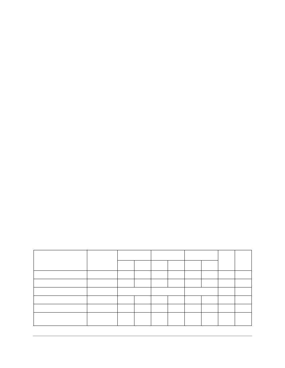
Table 9. L2CLK Output AC Timing Specications
At recommended operating conditions (see Table 3)
Parameter
Symbol
400 MHz
450 MHz
500 MHz
Unit
Notes
Min
Max
Min
Max
Min
Max
L2CLK frequency
fL2CLK
133
400
133
400
133
400
MHz
1, 4
L2CLK cycle time
tL2CLK
2.5
7.5
2.5
7.5
2.5
7.5
ns
L2CLK duty cycle
tCHCL/tL2CLK
50
%
2
Internal DLL-relock time
640
—
640
—
640
—
L2CLK
3
DLL capture window
0
10
0
10
0
10
ns
5
L2CLK_OUT
output-to-output skew
tL2CSKW
—50—50—50
ps
6
相关PDF资料 |
PDF描述 |
|---|---|
| MC68HC908QY4CP | 8-BIT, FLASH, 8 MHz, MICROCONTROLLER, PDIP16 |
| MC68HC908QY4MDT | 8-BIT, FLASH, 8 MHz, MICROCONTROLLER, PDSO16 |
| MC68HC908QY4MDW | 8-BIT, FLASH, 8 MHz, MICROCONTROLLER, PDSO16 |
| MC68HC908QY4MP | 8-BIT, FLASH, 8 MHz, MICROCONTROLLER, PDIP16 |
| MC68LK332ACFC16 | 32-BIT, 16.78 MHz, MICROCONTROLLER, PQFP132 |
相关代理商/技术参数 |
参数描述 |
|---|---|
| MPC7410VS400LE | 功能描述:微处理器 - MPU NITRO R1.4 105C PB FREE RoHS:否 制造商:Atmel 处理器系列:SAMA5D31 核心:ARM Cortex A5 数据总线宽度:32 bit 最大时钟频率:536 MHz 程序存储器大小:32 KB 数据 RAM 大小:128 KB 接口类型:CAN, Ethernet, LIN, SPI,TWI, UART, USB 工作电源电压:1.8 V to 3.3 V 最大工作温度:+ 85 C 安装风格:SMD/SMT 封装 / 箱体:FBGA-324 |
| MPC7410VS400NE | 功能描述:微处理器 - MPU REV 1.4 105C LGA RoHS:否 制造商:Atmel 处理器系列:SAMA5D31 核心:ARM Cortex A5 数据总线宽度:32 bit 最大时钟频率:536 MHz 程序存储器大小:32 KB 数据 RAM 大小:128 KB 接口类型:CAN, Ethernet, LIN, SPI,TWI, UART, USB 工作电源电压:1.8 V to 3.3 V 最大工作温度:+ 85 C 安装风格:SMD/SMT 封装 / 箱体:FBGA-324 |
| MPC7410VS450LE | 功能描述:微处理器 - MPU NITRO R1.4 105C PB FREE RoHS:否 制造商:Atmel 处理器系列:SAMA5D31 核心:ARM Cortex A5 数据总线宽度:32 bit 最大时钟频率:536 MHz 程序存储器大小:32 KB 数据 RAM 大小:128 KB 接口类型:CAN, Ethernet, LIN, SPI,TWI, UART, USB 工作电源电压:1.8 V to 3.3 V 最大工作温度:+ 85 C 安装风格:SMD/SMT 封装 / 箱体:FBGA-324 |
| MPC7410VS450NE | 功能描述:微处理器 - MPU REV 1.4 105C LGA RoHS:否 制造商:Atmel 处理器系列:SAMA5D31 核心:ARM Cortex A5 数据总线宽度:32 bit 最大时钟频率:536 MHz 程序存储器大小:32 KB 数据 RAM 大小:128 KB 接口类型:CAN, Ethernet, LIN, SPI,TWI, UART, USB 工作电源电压:1.8 V to 3.3 V 最大工作温度:+ 85 C 安装风格:SMD/SMT 封装 / 箱体:FBGA-324 |
| MPC7410VS500LE | 功能描述:微处理器 - MPU NITRO R1.4 105C PB FREE RoHS:否 制造商:Atmel 处理器系列:SAMA5D31 核心:ARM Cortex A5 数据总线宽度:32 bit 最大时钟频率:536 MHz 程序存储器大小:32 KB 数据 RAM 大小:128 KB 接口类型:CAN, Ethernet, LIN, SPI,TWI, UART, USB 工作电源电压:1.8 V to 3.3 V 最大工作温度:+ 85 C 安装风格:SMD/SMT 封装 / 箱体:FBGA-324 |
发布紧急采购,3分钟左右您将得到回复。