- 您现在的位置:买卖IC网 > PDF目录4042 > MPC8266AZUPJDC (Freescale Semiconductor)IC MPU POWERQUICC II 480-TBGA PDF资料下载
参数资料
| 型号: | MPC8266AZUPJDC |
| 厂商: | Freescale Semiconductor |
| 文件页数: | 44/50页 |
| 文件大小: | 0K |
| 描述: | IC MPU POWERQUICC II 480-TBGA |
| 标准包装: | 21 |
| 系列: | MPC82xx |
| 处理器类型: | 32-位 MPC82xx PowerQUICC II |
| 速度: | 300MHz |
| 电压: | 2V |
| 安装类型: | 表面贴装 |
| 封装/外壳: | 480-LBGA |
| 供应商设备封装: | 408-TBGA(37.5x37.5) |
| 包装: | 托盘 |
第1页第2页第3页第4页第5页第6页第7页第8页第9页第10页第11页第12页第13页第14页第15页第16页第17页第18页第19页第20页第21页第22页第23页第24页第25页第26页第27页第28页第29页第30页第31页第32页第33页第34页第35页第36页第37页第38页第39页第40页第41页第42页第43页当前第44页第45页第46页第47页第48页第49页第50页
MPC8260A PowerQUICC II Integrated Communications Processor Hardware Specifications, Rev. 2.0
Freescale Semiconductor
49
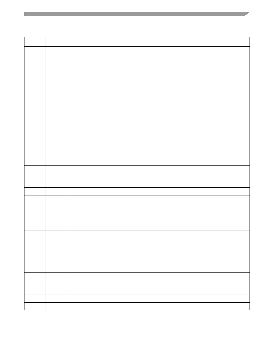
Document Revision History
0.9
8/2003
Note: In revision 0.3, sp30 (Table 10) was changed. This change was not previously recorded in this
“Document Revision History” Table.
Removal of “HiP4 PowerQUICC II Documentation” table. These supplemental specifications have
been replaced by revision 1 of the
MPC8260 PowerQUICC II Family Reference Manual.
Figure 1 and Section 1, “Features”: Addition of MPC8255 notes
Addition of Figure 2
Addition of VCCSYN to “Note: Core, PLL, and I/O Supply Voltages” following Table 2
Addition of note 1 to Table 3
Table 4: Changes to
θJA and θJB and θJC.
Table 9: Change of sp10.
Addition of Table 15.
Table 21: Addition of FCC2 Rx and Tx [3,4] to CPM pins PD7, PD18, PD19, and PD29. Also, the
addition of SPICLK to PC19. They are documented correctly in the parallel I/O ports chapter in the
MPC8260 PowerQUICC II Family Reference Manual but had previously been omitted from
0.8
1/2003
Table 2: Modification to supply voltage ranges reflected in notes 2, 3, and 4.
Table 4: Addition of
θJB and θJC.
0.7
5/2002
Section 1, “Features”: minimum supported core frequency of 150 MHz
Section 1, “Features”: updated performance values (under “Dual-issue integer core”)
Table 2: Note 2 (changes in italics): “...
less than or equal to 233 MHz, 166 MHz CPM...”
Table 2: Addition of note 3.
0.6
3/2002
Table 21: Modified notes to pins AE11 and AF25.
0.5
3/2002
Table 21: Modified notes to pins AE11 and AF25.
Table 21: Addition of note to pins AA1 and AG4 (Therm0 and Therm1).
0.4
2/2002
Note 2 for Table 2 (changes in italics): “...greater than
or equal to 266 MHz, 200 MHz CPM...”
Table 19: Core and bus frequency values for the following ranges of MODCK_HMODCK: 0011_000
to 0011_100 and 1011_000 to 1011_1000
Table 21: Notes added to pins at AE11, AF25, U5, and V4.
0.3
11/2001
Table 1: note 3
Section 2.1: Removal of “Warning” recommending use of bootstrap diodes. They are not needed.
Table 9: Change to sp12.
Table 10: Change to sp32.
Addition of note at beginning of Section 3.2
Table 21: Additions to B27, C28, D25, D27, E26, G29, H26–28, N25, P29, AF25, AA25, AB27
0.2
11/2001
Revision of Table 5, “Power Dissipation”
Modification to pinout diagram, Figure 13
Additional revisions to text and figures throughout
0.1
8/2001
Table 8: Change to sp20/sp21.
0
—
Initial version
Table 23. Document Revision History (continued)
Revision
Date
Substantive Changes
相关PDF资料 |
PDF描述 |
|---|---|
| ACB108DHAD | CONN EDGECARD 216PS R/A .050 DIP |
| MC68EN360CRC25L | IC MPU QUICC 32BIT 25MHZ 241-PGA |
| MPC8545EVTATGB | MPU POWERQUICC III 783-PBGA |
| XPC8260ZUHFBC | IC MPU POWERQUICC II 480-TBGA |
| FMC31DREF-S734 | CONN EDGECARD 62POS .100 EYELET |
相关代理商/技术参数 |
参数描述 |
|---|---|
| MPC8266CVR | 制造商:MOTOROLA 制造商全称:Motorola, Inc 功能描述:MPC826xA (HiP4) Family Hardware Specifications |
| MPC8266CZU | 制造商:MOTOROLA 制造商全称:Motorola, Inc 功能描述:MPC826xA (HiP4) Family Hardware Specifications |
| MPC8266VR | 制造商:MOTOROLA 制造商全称:Motorola, Inc 功能描述:MPC826xA (HiP4) Family Hardware Specifications |
| MPC8266ZU | 制造商:MOTOROLA 制造商全称:Motorola, Inc 功能描述:MPC826xA (HiP4) Family Hardware Specifications |
| MPC826XA | 制造商:MOTOROLA 制造商全称:Motorola, Inc 功能描述:Hardware Specifications |
发布紧急采购,3分钟左右您将得到回复。