- 您现在的位置:买卖IC网 > PDF目录45358 > MPC8270CZUUPEA (FREESCALE SEMICONDUCTOR INC) 32-BIT, 100 MHz, RISC PROCESSOR, PBGA480 PDF资料下载
参数资料
| 型号: | MPC8270CZUUPEA |
| 厂商: | FREESCALE SEMICONDUCTOR INC |
| 元件分类: | 微控制器/微处理器 |
| 英文描述: | 32-BIT, 100 MHz, RISC PROCESSOR, PBGA480 |
| 封装: | 37 X 37 MM, 1.27 MM PITCH, FTBGA-480 |
| 文件页数: | 124/156页 |
| 文件大小: | 1680K |
| 代理商: | MPC8270CZUUPEA |
第1页第2页第3页第4页第5页第6页第7页第8页第9页第10页第11页第12页第13页第14页第15页第16页第17页第18页第19页第20页第21页第22页第23页第24页第25页第26页第27页第28页第29页第30页第31页第32页第33页第34页第35页第36页第37页第38页第39页第40页第41页第42页第43页第44页第45页第46页第47页第48页第49页第50页第51页第52页第53页第54页第55页第56页第57页第58页第59页第60页第61页第62页第63页第64页第65页第66页第67页第68页第69页第70页第71页第72页第73页第74页第75页第76页第77页第78页第79页第80页第81页第82页第83页第84页第85页第86页第87页第88页第89页第90页第91页第92页第93页第94页第95页第96页第97页第98页第99页第100页第101页第102页第103页第104页第105页第106页第107页第108页第109页第110页第111页第112页第113页第114页第115页第116页第117页第118页第119页第120页第121页第122页第123页当前第124页第125页第126页第127页第128页第129页第130页第131页第132页第133页第134页第135页第136页第137页第138页第139页第140页第141页第142页第143页第144页第145页第146页第147页第148页第149页第150页第151页第152页第153页第154页第155页第156页
MOTOROLA
MPC8280 PowerQUICC II Family Hardware Specications
7
Operating Conditions
– Independent transmit and receive routing, frame synchronization
– Supports T1, CEPT, T1/E1, T3/E3, pulse code modulation highway, ISDN basic rate, ISDN
primary rate, Motorola interchip digital link (IDL), general circuit interface (GCI), and
user-dened TDM serial interfaces
— Eight independent baud rate generators and 20 input clock pins for supplying clocks to FCCs,
SCCs, SMCs, and serial channels
— Four independent 16-bit timers that can be interconnected as two 32-bit timers
Inverse multiplexing for ATM capabilities (IMA) (MPC8280 only).Supported by eight transfer
transmission convergence (TC) layers between the TDMs and FCC2.
Transmission convergence (TC) layer (MPC8280 only)
2
Operating Conditions
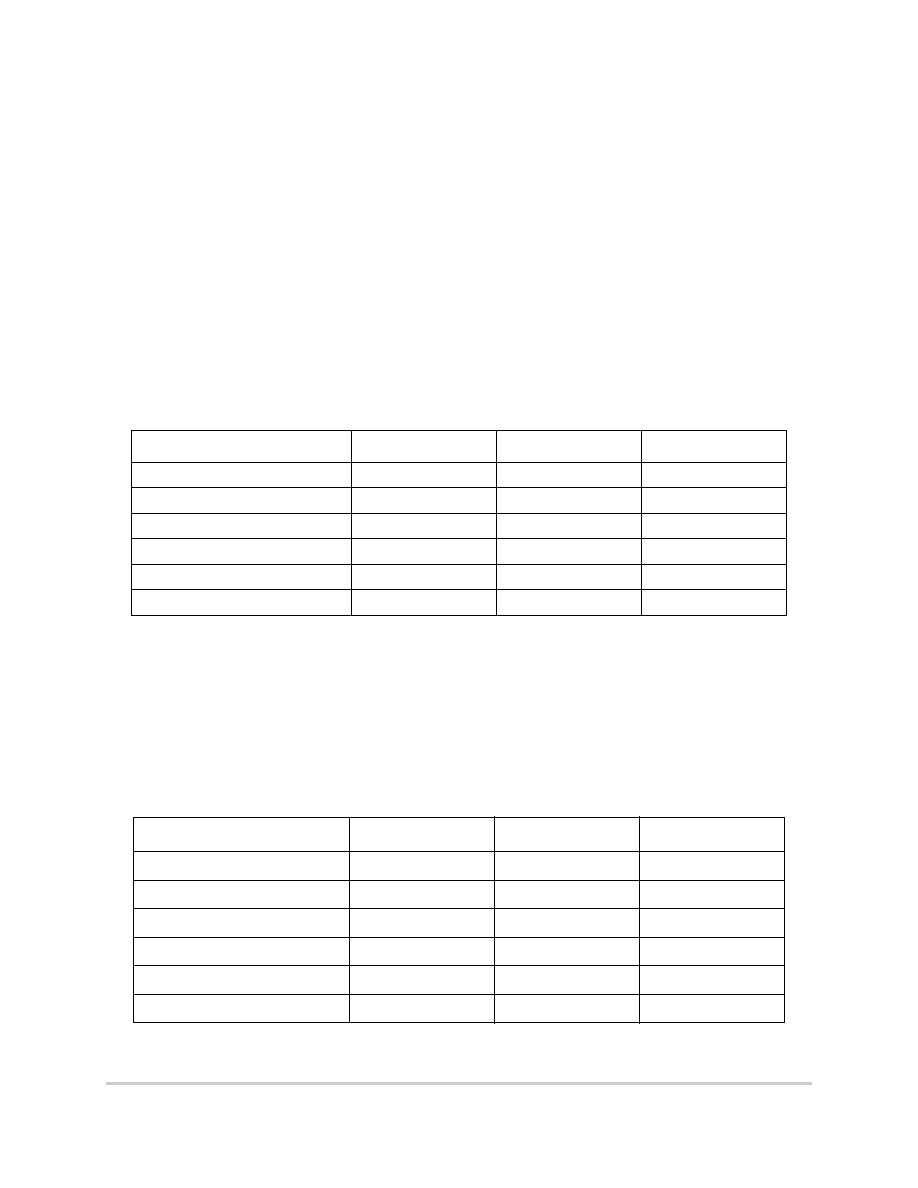
Table 3 shows the maximum electrical ratings.
Table 4 lists recommended operational voltage conditions.
Table 3. Absolute Maximum Ratings1
1 Absolute maximum ratings are stress ratings only; functional operation (see Table 4) at the maximums is not
guaranteed. Stress beyond those listed may affect device reliability or cause permanent damage.
Rating
Symbol
Value
Unit
Core supply voltage2
2 Caution: VDD/VCCSYN must not exceed VDDH by more than 0.4 V at any time, including during power-on
reset.
VDD
-0.3 – 2.25
V
PLL supply voltage2
VCCSYN
-0.3 – 2.25
V
I/O supply voltage3
3 Caution:VDDH can exceed VDD/VCCSYN by 3.3 V during power on reset by no more than 100 mSec.VDDH
should not exceed VDD/VCCSYN by more than 2.5 V during normal operation.
VDDH
-0.3 – 4.0
V
Input voltage4
4 Caution: VIN must not exceed VDDH by more than 2.5 V at any time, including during power-on reset.
VIN
GND(-0.3) – 3.6
V
Junction temperature
Tj
120
C
Storage temperature range
TSTG
(-55) – (+150)
C
Table 4. Recommended Operating Conditions1
1 Caution: These are the recommended and tested operating conditions. Proper operation outside of these
conditions is not guaranteed.
Rating
Symbol
Value
Unit
Core supply voltage
VDD
1.45 – 1.60
V
PLL supply voltage
VCCSYN
1.45 – 1.60
V
I/O supply voltage
VDDH
3.135 – 3.465
V
Input voltage
VIN
GND (-0.3) – 3.465
V
Junction temperature (maximum)
Tj
1052
C
Ambient temperature
TA
C
F
re
e
sc
a
le
S
e
m
ic
o
n
d
u
c
to
r,
I
Freescale Semiconductor, Inc.
For More Information On This Product,
Go to: www.freescale.com
n
c
..
.
相关PDF资料 |
PDF描述 |
|---|---|
| MPC8275CZQMIBA | 32-BIT, 66.67 MHz, RISC PROCESSOR, PBGA516 |
| MPC8270ZQMIBA | 32-BIT, 66.67 MHz, RISC PROCESSOR, PBGA516 |
| MPC8280CZUUPE | 32-BIT, 100 MHz, RISC PROCESSOR, PBGA480 |
| MPC8275ZQMIBA | 32-BIT, 66.67 MHz, RISC PROCESSOR, PBGA516 |
| MPC8280CZQMIBX | 32-BIT, 266 MHz, RISC PROCESSOR, PBGA516 |
相关代理商/技术参数 |
参数描述 |
|---|---|
| MPC8270VR | 制造商:MOTOROLA 制造商全称:Motorola, Inc 功能描述:PowerQUICC II Family Hardware Specifications |
| MPC8270VRB | 制造商:FREESCALE 制造商全称:Freescale Semiconductor, Inc 功能描述:PowerQUICC II⑩ Family Hardware Specifications |
| MPC8270VRE | 制造商:FREESCALE 制造商全称:Freescale Semiconductor, Inc 功能描述:PowerQUICC II⑩ Family Hardware Specifications |
| MPC8270VRI | 制造商:FREESCALE 制造商全称:Freescale Semiconductor, Inc 功能描述:PowerQUICC II⑩ Family Hardware Specifications |
| MPC8270VRM | 制造商:FREESCALE 制造商全称:Freescale Semiconductor, Inc 功能描述:PowerQUICC II⑩ Family Hardware Specifications |
发布紧急采购,3分钟左右您将得到回复。