- 您现在的位置:买卖IC网 > PDF目录4075 > MPC8323ZQADDC (Freescale Semiconductor)IC MPU PWRQUICC II 516-PBGA PDF资料下载
参数资料
| 型号: | MPC8323ZQADDC |
| 厂商: | Freescale Semiconductor |
| 文件页数: | 20/82页 |
| 文件大小: | 0K |
| 描述: | IC MPU PWRQUICC II 516-PBGA |
| 产品培训模块: | MPC8323E PowerQUICC II Pro Processor |
| 标准包装: | 40 |
| 系列: | MPC83xx |
| 处理器类型: | 32-位 MPC83xx PowerQUICC II Pro |
| 速度: | 266MHz |
| 电压: | 1V |
| 安装类型: | 表面贴装 |
| 封装/外壳: | 516-BBGA |
| 供应商设备封装: | 516-FPBGA(27x27) |
| 包装: | 托盘 |
| 配用: | MPC8323E-RDB-ND - BOARD REFERENCE DESIGN |
第1页第2页第3页第4页第5页第6页第7页第8页第9页第10页第11页第12页第13页第14页第15页第16页第17页第18页第19页当前第20页第21页第22页第23页第24页第25页第26页第27页第28页第29页第30页第31页第32页第33页第34页第35页第36页第37页第38页第39页第40页第41页第42页第43页第44页第45页第46页第47页第48页第49页第50页第51页第52页第53页第54页第55页第56页第57页第58页第59页第60页第61页第62页第63页第64页第65页第66页第67页第68页第69页第70页第71页第72页第73页第74页第75页第76页第77页第78页第79页第80页第81页第82页
MPC8323E PowerQUICC II Pro Integrated Communications Processor Family Hardware Specifications, Rev. 4
Freescale Semiconductor
27
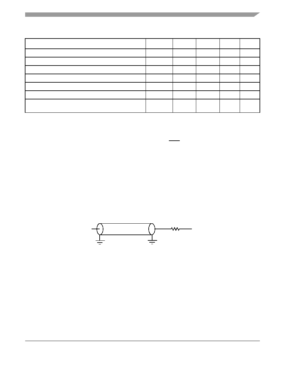
Local Bus
Figure 14 provides the AC test load for the local bus.
Figure 14. Local Bus C Test Load
LALE output fall to LAD output transition (LATCH hold time)
tLBOTOT2
3—
ns
6
LALE output fall to LAD output transition (LATCH hold time)
tLBOTOT3
2.5
—
ns
7
Local bus clock (LCLK
n) to output valid
tLBKHOV
—3
ns
3
Local bus clock (LCLK
n) to output high impedance for LAD/LDP
tLBKHOZ
—4
ns
8
Local bus clock (LCLK
n) duty cycle
tLBDC
47
53
%
—
Local bus clock (LCLK
n) jitter specification
tLBRJ
—
400
ps
—
Delay between the input clock (PCI_SYNC_IN) of local bus
output clock (LCLK
n)
tLBCDL
—1.7
ns
—
Notes:
1. The symbols used for timing specifications follow the pattern of t(first two letters of functional block)(signal)(state)(reference)(state) for
inputs and t(first two letters of functional block)(reference)(state)(signal)(state) for outputs. For example, tLBIXKH1 symbolizes local bus
timing (LB) for the input (I) to go invalid (X) with respect to the time the tLBK clock reference (K) goes high (H), in this case for
clock one(1).
2. All timings are in reference to falling edge of LCLK0 (for all outputs and for LGTA and LUPWAIT inputs) or rising edge of
LCLK0 (for all other inputs).
3. All signals are measured from OVDD/2 of the rising/falling edge of LCLK0 to 0.4 × OVDD of the signal in question for 3.3-V
signaling levels.
4. Input timings are measured at the pin.
5. tLBOTOT1 should be used when RCWH[LALE] is not set and the load on LALE output pin is at least 10 pF less than the load
on LAD output pins.
6. tLBOTOT2 should be used when RCWH[LALE] is set and the load on LALE output pin is at least 10 pF less than the load on
LAD output pins.
7. tLBOTOT3 should be used when RCWH[LALE] is set and the load on LALE output pin equals to the load on LAD output pins.
8. For purposes of active/float timing measurements, the Hi-Z or off state is defined to be when the total current delivered
through the component pin is less than or equal to the leakage current specification.
Table 30. Local Bus General Timing Parameters (continued)
Parameter
Symbol1
Min
Max
Unit
Notes
Output
Z0 = 50 Ω
OVDD/2
RL = 50 Ω
相关PDF资料 |
PDF描述 |
|---|---|
| IDT709269S15PF8 | IC SRAM 256KBIT 15NS 100TQFP |
| IDT709359L9PF8 | IC SRAM 144KBIT 9NS 100TQFP |
| IDT709169L9PF8 | IC SRAM 144KBIT 9NS 100TQFP |
| MPC8323VRADDC | IC MPU PWRQUICC II 516-PBGA |
| MPC875CVR66 | IC MPU POWERQUICC 66MHZ 256PBGA |
相关代理商/技术参数 |
参数描述 |
|---|---|
| MPC8323ZQADDCA | 制造商:FREESCALE 制造商全称:Freescale Semiconductor, Inc 功能描述:PowerQUICC? II Pro Integrated Communications Processor Family Hardware Specifications |
| MPC8323ZQAFDC | 功能描述:微处理器 - MPU 8323 PBGA W/O ENCR RoHS:否 制造商:Atmel 处理器系列:SAMA5D31 核心:ARM Cortex A5 数据总线宽度:32 bit 最大时钟频率:536 MHz 程序存储器大小:32 KB 数据 RAM 大小:128 KB 接口类型:CAN, Ethernet, LIN, SPI,TWI, UART, USB 工作电源电压:1.8 V to 3.3 V 最大工作温度:+ 85 C 安装风格:SMD/SMT 封装 / 箱体:FBGA-324 |
| MPC8323ZQAFDCA | 制造商:FREESCALE 制造商全称:Freescale Semiconductor, Inc 功能描述:PowerQUICC? II Pro Integrated Communications Processor Family Hardware Specifications |
| MPC832XE-MDS-PB | 功能描述:开发板和工具包 - 其他处理器 PROCESSOR BOARD (SOCKET) RoHS:否 制造商:Freescale Semiconductor 产品:Development Systems 工具用于评估:P3041 核心:e500mc 接口类型:I2C, SPI, USB 工作电源电压: |
| MPC8343CVRADD | 功能描述:IC MPU PWRQUICC II PRO 620-PBGA RoHS:是 类别:集成电路 (IC) >> 嵌入式 - 微处理器 系列:MPC83xx 标准包装:1 系列:MPC85xx 处理器类型:32-位 MPC85xx PowerQUICC III 特点:- 速度:1.2GHz 电压:1.1V 安装类型:表面贴装 封装/外壳:783-BBGA,FCBGA 供应商设备封装:783-FCPBGA(29x29) 包装:托盘 |
发布紧急采购,3分钟左右您将得到回复。