- 您现在的位置:买卖IC网 > PDF目录80544 > MPC8349VVALDMPC8349ZUAGD (FREESCALE SEMICONDUCTOR INC) 32-BIT, 667 MHz, MICROPROCESSOR, PBGA672 PDF资料下载
参数资料
| 型号: | MPC8349VVALDMPC8349ZUAGD |
| 厂商: | FREESCALE SEMICONDUCTOR INC |
| 元件分类: | 微控制器/微处理器 |
| 英文描述: | 32-BIT, 667 MHz, MICROPROCESSOR, PBGA672 |
| 封装: | 35 X 35 MM, 1.46 MM HEIGHT, 1 MM PITCH, LEAD FREE, TBGA-672 |
| 文件页数: | 62/108页 |
| 文件大小: | 1275K |
| 代理商: | MPC8349VVALDMPC8349ZUAGD |
第1页第2页第3页第4页第5页第6页第7页第8页第9页第10页第11页第12页第13页第14页第15页第16页第17页第18页第19页第20页第21页第22页第23页第24页第25页第26页第27页第28页第29页第30页第31页第32页第33页第34页第35页第36页第37页第38页第39页第40页第41页第42页第43页第44页第45页第46页第47页第48页第49页第50页第51页第52页第53页第54页第55页第56页第57页第58页第59页第60页第61页当前第62页第63页第64页第65页第66页第67页第68页第69页第70页第71页第72页第73页第74页第75页第76页第77页第78页第79页第80页第81页第82页第83页第84页第85页第86页第87页第88页第89页第90页第91页第92页第93页第94页第95页第96页第97页第98页第99页第100页第101页第102页第103页第104页第105页第106页第107页第108页
MPC8349E PowerQUICC II Pro Integrated Host Processor Hardware Specifications, Rev. 7
Freescale Semiconductor
57
I2C
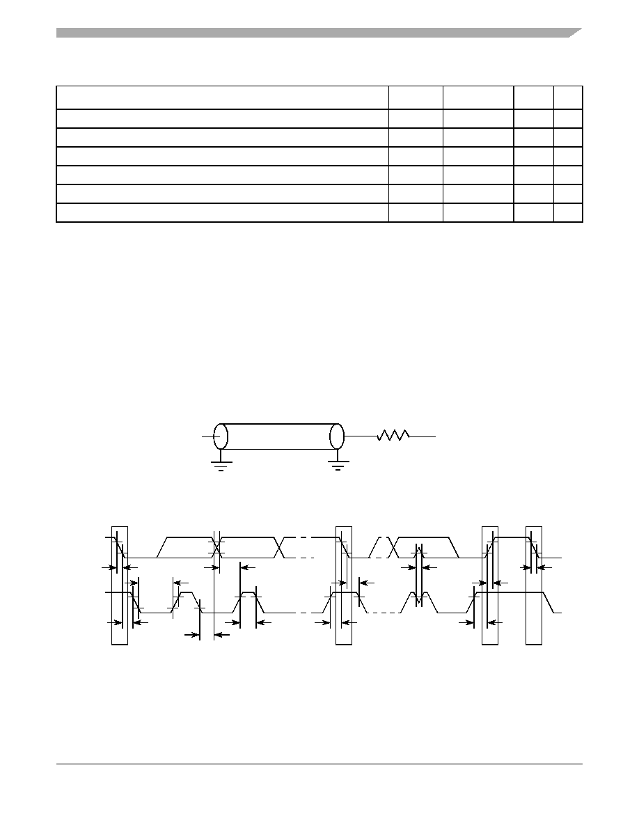
Figure 30. I2C AC Test Load
Figure 31. I2C Bus AC Timing Diagram
Rise time of both SDA and SCL signals
tI2CR
20 + 0.1 Cb
4
300
ns
Fall time of both SDA and SCL signals
tI2CF
20 + 0.1 Cb
4
300
ns
Set-up time for STOP condition
tI2PVKH
0.6
—
μs
Bus free time between a STOP and START condition
tI2KHDX
1.3
—
μs
Noise margin at the LOW level for each connected device (including hysteresis)
VNL
0.1
× OV
DD
—V
Noise margin at the HIGH level for each connected device (including hysteresis)
VNH
0.2
× OV
DD
—V
Notes:
1. The symbols for timing specifications follow the pattern of t(first two letters of functional block)(signal)(state) (reference)(state) for inputs
and t(first two letters of functional block)(reference)(state)(signal)(state) for outputs. For example, tI2DVKH symbolizes I
2C timing (I2) with
respect to the time data input signals (D) reach the valid state (V) relative to the tI2C clock reference (K) going to the high (H)
state or setup time. Also, tI2SXKL symbolizes I
2C timing (I2) for the time that the data with respect to the start condition (S)
goes invalid (X) relative to the tI2C clock reference (K) going to the low (L) state or hold time. Also, tI2PVKH symbolizes I
2C
timing (I2) for the time that the data with respect to the stop condition (P) reaches the valid state (V) relative to the tI2C clock
reference (K) going to the high (H) state or setup time. For rise and fall times, the latter convention is used with the appropriate
letter: R (rise) or F (fall).
2. MPC8349E provides a hold time of at least 300 ns for the SDA signal (referred to the VIHmin of the SCL signal) to bridge the
undefined region of the falling edge of SCL.
3. The maximum tI2DVKH must be met only if the device does not stretch the LOW period (tI2CL) of the SCL signal.
4. CB = capacitance of one bus line in pF.
Table 39. I2C AC Electrical Specifications (continued)
Parameter
Symbol 1
Min
Max
Unit
Output
Z0 = 50 Ω
OVDD/2
RL = 50 Ω
Sr
S
SDA
SCL
tI2CF
tI2SXKL
tI2CL
tI2CH
tI2DXKL
tI2DVKH
tI2SXKL
tI2SVKH
tI2KHKL
tI2PVKH
tI2CR
tI2CF
PS
相关PDF资料 |
PDF描述 |
|---|---|
| MCAQE16GQAPR-MWA | FLASH MEMORY DRIVE CONTROLLER, PBGA |
| MB96F379RWBPMC-GSE2 | 16-BIT, FLASH, 56 MHz, MICROCONTROLLER, PQFP144 |
| MPC8543VTANGA | 32-BIT, 800 MHz, MICROPROCESSOR, PBGA783 |
| MAX7391AXWB | 16 MHz, OTHER CLOCK GENERATOR, PDSO8 |
| MAX7391CJRD | 4 MHz, OTHER CLOCK GENERATOR, PDSO8 |
相关代理商/技术参数 |
参数描述 |
|---|---|
| MPC8349VVALFB | 功能描述:微处理器 - MPU 8349 TBGA NO-PB W/O ENC RoHS:否 制造商:Atmel 处理器系列:SAMA5D31 核心:ARM Cortex A5 数据总线宽度:32 bit 最大时钟频率:536 MHz 程序存储器大小:32 KB 数据 RAM 大小:128 KB 接口类型:CAN, Ethernet, LIN, SPI,TWI, UART, USB 工作电源电压:1.8 V to 3.3 V 最大工作温度:+ 85 C 安装风格:SMD/SMT 封装 / 箱体:FBGA-324 |
| MPC8349ZUAGD | 功能描述:IC MPU PWRQUICC II PRO 672-TBGA RoHS:否 类别:集成电路 (IC) >> 嵌入式 - 微处理器 系列:MPC83xx 标准包装:1 系列:MPC85xx 处理器类型:32-位 MPC85xx PowerQUICC III 特点:- 速度:1.2GHz 电压:1.1V 安装类型:表面贴装 封装/外壳:783-BBGA,FCBGA 供应商设备封装:783-FCPBGA(29x29) 包装:托盘 |
| MPC8349ZUAGDB | 功能描述:微处理器 - MPU 8349 TBGA W/O ENCRYP RoHS:否 制造商:Atmel 处理器系列:SAMA5D31 核心:ARM Cortex A5 数据总线宽度:32 bit 最大时钟频率:536 MHz 程序存储器大小:32 KB 数据 RAM 大小:128 KB 接口类型:CAN, Ethernet, LIN, SPI,TWI, UART, USB 工作电源电压:1.8 V to 3.3 V 最大工作温度:+ 85 C 安装风格:SMD/SMT 封装 / 箱体:FBGA-324 |
| MPC8349ZUAGFB | 制造商:FREESCALE 制造商全称:Freescale Semiconductor, Inc 功能描述:Integrated Host Processor Hardware Specifications |
| MPC8349ZUAJD | 功能描述:IC MPU PWRQUICC II PRO 672-TBGA RoHS:是 类别:集成电路 (IC) >> 嵌入式 - 微处理器 系列:MPC83xx 标准包装:1 系列:MPC85xx 处理器类型:32-位 MPC85xx PowerQUICC III 特点:- 速度:1.2GHz 电压:1.1V 安装类型:表面贴装 封装/外壳:783-BBGA,FCBGA 供应商设备封装:783-FCPBGA(29x29) 包装:托盘 |
发布紧急采购,3分钟左右您将得到回复。